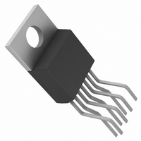
LT1210CT7 Linear Technology, LT1210CT7 Datasheet - Page 10

LT1210CT7
Manufacturer Part Number
LT1210CT7
Description
IC AMP C-FEEDBACK 1.1A TO-220-7
Manufacturer
Linear Technology
Datasheet
1.LT1210CT7PBF.pdf
(16 pages)
Specifications of LT1210CT7
Amplifier Type
Current Feedback
Number Of Circuits
1
Slew Rate
90 V/µs
-3db Bandwidth
55MHz
Current - Input Bias
10µA
Voltage - Input Offset
3000µV
Current - Supply
35mA
Current - Output / Channel
2A
Voltage - Supply, Single/dual (±)
10 V ~ 30 V, ±5 V ~ 15 V
Operating Temperature
0°C ~ 70°C
Mounting Type
Through Hole
Package / Case
TO-220-7 (Bent and Staggered Leads)
Lead Free Status / RoHS Status
Contains lead / RoHS non-compliant
Output Type
-
Gain Bandwidth Product
-
Available stocks
Company
Part Number
Manufacturer
Quantity
Price
Company:
Part Number:
LT1210CT7
Manufacturer:
XI;
Quantity:
5 510
Part Number:
LT1210CT7
Manufacturer:
LT
Quantity:
20 000
Part Number:
LT1210CT7#06PBF
Manufacturer:
LINEAR/凌特
Quantity:
20 000
Part Number:
LT1210CT7#37PBF
Manufacturer:
LINEAR/凌特
Quantity:
20 000
Part Number:
LT1210CT7#44PBF
Manufacturer:
LINEAR/凌特
Quantity:
20 000
Company:
Part Number:
LT1210CT7#PBF
Manufacturer:
LINEAR
Quantity:
1 250
Part Number:
LT1210CT7#PBF
Manufacturer:
LINEAR/凌特
Quantity:
20 000
LT1210
the bandwidth is reduced. The photos in Figures 5a, 5b and
5c show the large-signal response of the LT1210 for
various gain configurations. The slew rate varies from
770V/µs for a gain of 1, to 1100V/µs for a gain of – 1.
A
10
PPLICATI
Figure 5c. Large-Signal Response, A
Figure 5b. Large-Signal Response, A
Figure 5a. Large-Signal Response, A
R
R
R
R
R
R
F
L
F
L
F
L
= R
= 10Ω
= 825Ω
= 10Ω
= R
= 10Ω
G
G
= 750Ω
= 750Ω
O
U
V
S
S
= ±15V
V
S
V
= ±15V
S
I FOR ATIO
= ±15V
U
W
V
1210 F05a
V
1210 F05b
V
1210 F05c
= 2
= –1
= 1
U
When the LT1210 is used to drive capacitive loads, the
available output current can limit the overall slew rate. In
the fastest configuration, the LT1210 is capable of a slew
rate of over 1V/ns. The current required to slew a capacitor
at this rate is 1mA per picofarad of capacitance, so
10,000pF would require 10A! The photo (Figure 6) shows
the large-signal behavior with C
rate is about 150V/µs, determined by the current limit of
1.5A.
Differential Input Signal Swing
The differential input swing is limited to about ±6V by an
ESD protection device connected between the inputs. In
normal operation, the differential voltage between the
input pins is small, so this clamp has no effect; however,
in the shutdown mode the differential swing can be the
same as the input swing. The clamp voltage will then set
the maximum allowable input voltage. To allow for some
margin, it is recommended that the input signal be less
than ±5V when the device is shut down.
Capacitance on the Inverting Input
Current feedback amplifiers require resistive feedback
from the output to the inverting input for stable operation.
Take care to minimize the stray capacitance between the
output and the inverting input. Capacitance on the invert-
ing input to ground will cause peaking in the frequency
response (and overshoot in the transient response), but it
does not degrade the stability of the amplifier.
Figure 6. Large-Signal Response, C
R
R
F
L
= R
=
∞
G
= 3k
V
S
= ±15V
L
= 10,000pF. The slew
L
= 10,000pF
1210 F06
1210fa


