LT1210CT7 Linear Technology, LT1210CT7 Datasheet - Page 3
LT1210CT7
Manufacturer Part Number
LT1210CT7
Description
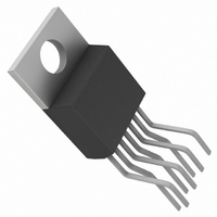
IC AMP C-FEEDBACK 1.1A TO-220-7
Manufacturer
Linear Technology
Datasheet
1.LT1210CT7PBF.pdf
(16 pages)
Specifications of LT1210CT7
Amplifier Type
Current Feedback
Number Of Circuits
1
Slew Rate
90 V/µs
-3db Bandwidth
55MHz
Current - Input Bias
10µA
Voltage - Input Offset
3000µV
Current - Supply
35mA
Current - Output / Channel
2A
Voltage - Supply, Single/dual (±)
10 V ~ 30 V, ±5 V ~ 15 V
Operating Temperature
0°C ~ 70°C
Mounting Type
Through Hole
Package / Case
TO-220-7 (Bent and Staggered Leads)
Lead Free Status / RoHS Status
Contains lead / RoHS non-compliant
Output Type
-
Gain Bandwidth Product
-
Available stocks
Company
Part Number
Manufacturer
Quantity
Price

Company:
Part Number:
LT1210CT7
Manufacturer:
XI;
Quantity:
5 510
Part Number:
LT1210CT7
Manufacturer:
LT
Quantity:
20 000
Part Number:
LT1210CT7#06PBF
Manufacturer:
LINEAR/凌特
Quantity:
20 000
Part Number:
LT1210CT7#37PBF
Manufacturer:
LINEAR/凌特
Quantity:
20 000
Part Number:
LT1210CT7#44PBF
Manufacturer:
LINEAR/凌特
Quantity:
20 000
Company:
Part Number:
LT1210CT7#PBF
Manufacturer:
LINEAR
Quantity:
1 250
Part Number:
LT1210CT7#PBF
Manufacturer:
LINEAR/凌特
Quantity:
20 000


temperature range, otherwise specifications are at T
otherwise noted.
Note 1: Stresses beyond those listed under Absolute Maximum Ratings
may cause permanent damage to the device. Exposure to any Absolute
Maximum Rating condition for extended periods may affect device
reliability and lifetime.
Note 2: Applies to short circuits to ground only. A short circuit between
the output and either supply may permanently damage the part when
operated on supplies greater than ±10V.
Note 3: Commercial grade parts are designed to operate over the
temperature range of – 40°C ≤ T
guaranteed beyond 0°C ≤ T
– 40°C ≤ T
SYMBOL
CMRR
PSRR
A
R
V
I
I
SR
BW
ELECTRICAL CHARACTERISTICS
OUT
S
V
OL
OUT
A
≤ 85°C are available on special request. Consult factory.
PARAMETER
Common Mode Rejection Ratio
Inverting Input Current
Common Mode Rejection
Power Supply Rejection Ratio
Noninverting Input Current
Power Supply Rejection
Inverting Input Current
Power Supply Rejection
Large-Signal Voltage Gain
Transresistance, ∆V
Maximum Output Voltage Swing
Maximum Output Current (Note 4)
Supply Current (Note 4)
Supply Current, R
Positive Supply Current, Shutdown
Output Leakage Current, Shutdown
Slew Rate (Note 6)
Slew Rate (Note 4)
Differential Gain (Notes 4, 7)
Differential Phase (Notes 4, 7)
Small-Signal Bandwidth
A
≤ 70°C. Industrial grade parts tested over
SD
A
OUT
= 51k (Notes 4, 5)
≤ 85°C, but are neither tested nor
/∆I
IN
–
CONDITIONS
V
V
V
V
V
V
V
T
R
V
V
T
R
V
V
T
T
V
T
T
V
V
T
T
V
V
A
R
A
R
A
A
A
A
A
A
A
A
S
S
S
S
S
S
S
L
S
S
L
S
S
S
S
S
S
S
V
F
V
F
= 25°C, V
= 25°C, V
= 25°C, V
= 25°C, V
= 25°C, V
= 25°C, V
= 25°C, A
= 25°C, A
= ±15V, V
= ±5V, V
= ±15V, V
= ±5V, V
= ±5V to ±15V
= ±5V to ±15V
= ±5V to ±15V
= 10Ω (Note 3)
= ±15V, V
= ±5V, V
= 10Ω (Note 3)
= ±15V, V
= ±5V, V
= ±15V, R
= ±15V, V
= ±15V, V
= ±15V, R
= ±15V, R
= 2, V
= R
= 2, V
= R
A
G
G
= 25°C. V
= 680Ω, R
= 576Ω, R
S
S
= ±15V, Peaking ≤ 1dB,
= ±15V, Peaking ≤ 1dB,
The
CM
CM
OUT
OUT
S
S
S
S
S
S
V
V
CM
CM
OUT
OUT
SD
SD
L
F
F
= ±15V, V
= ±15V, V
= ±15V, R
= ±5V, R
= ±15V, V
= ±15V
= 2, R
= 2, R
= 750Ω, R
= 750Ω, R
= 1Ω
= ±2V
= ±2V
= ±2V, R
= ±2V, R
= 15V
●
= 15V
= ±12V
= ±12V
= ±8.5V, R
= ±8.5V, R
CM
denotes specifications which apply over the full operating
L
L
L
L
= 100Ω
= 10Ω
= 0V, ±5V ≤ V
= 400Ω
= 10Ω
L
OUT
OUT
SD
L
Note 4: SO package is recommended for ±5V supplies only, as the power
dissipation of the SO package limits performance on higher supplies. For
supply voltages greater than ±5V, use the TO-220 or DD package. See
“Thermal Considerations” in the Applications Information section for
details on calculating junction temperature. If the maximum dissipation of
the package is exceeded, the device will go into thermal shutdown.
Note 5: R
Note 6: Slew rate is measured at ±5V on a ±10V output signal while
operating on ±15V supplies with R
Note 7: NTSC composite video with an output level of 2V.
= 10Ω
L
L
G
G
= 10Ω (Note 3)
= 10Ω
= 10Ω
= 0V
= 750Ω, R
= 750Ω, R
L
L
= ±10V,
= ±10V,
= 10Ω (Note 3)
= 10Ω (Note 3)
SD
is connected between the Shutdown pin and ground.
S
L
L
≤ ±15V, pulse tested, V
= 15Ω
= 15Ω
●
●
●
●
●
●
●
●
●
●
●
●
●
●
●
●
●
±10.0
F
±2.5
±2.0
MIN
100
400
±8.5
1.1
55
50
60
55
55
55
75
75
= 1.5k, R
SD
±11.5
G
= 0V, unless
±3.0
TYP
260
200
200
900
900
0.1
0.1
0.7
2.0
0.3
0.1
62
60
77
30
71
68
68
35
15
55
35
= 1.5k and R
MAX
500
200
10
10
50
65
30
10
5
LT1210
L
= 400Ω.
UNITS
µA/V
µA/V
nA/V
µA/V
1210fa
3
V/µs
V/µs
MHz
MHz
DEG
mA
mA
mA
kΩ
kΩ
kΩ
dB
dB
dB
dB
dB
dB
µA
µA
%
V
V
V
V
A
Related parts for LT1210CT7
Image
Part Number
Description
Manufacturer
Datasheet
Request
R

Part Number:
Description:
1.1A/ 35MHz Current Feedback Amplifier
Manufacturer:
Linear Technology
Datasheet:
Part Number:
Description:
CD ROM LINEARVIEW DATASHEETS
Manufacturer:
Linear Technology

Part Number:
Description:
Standalone Linear Li-Ion Battery Charger with Thermal Regulation in ThinSOT
Manufacturer:
Linear Technology Corporation
Datasheet:
Part Number:
Description:
Low noise, high frequency, 8th order linear phase lowpass filter
Manufacturer:
Linear Technology Corporation
Datasheet:
Part Number:
Description:
Manufacturer:
Linear Technology Corporation
Datasheet:
Part Number:
Description:
Manufacturer:
Linear Technology Corporation
Datasheet:
Part Number:
Description:
Manufacturer:
Linear Technology Corporation
Datasheet:
Part Number:
Description:
Manufacturer:
Linear Technology Corporation
Datasheet:
Part Number:
Description:
Manufacturer:
Linear Technology Corporation
Datasheet:
Part Number:
Description:
Manufacturer:
Linear Technology Corporation
Datasheet:
Part Number:
Description:
Manufacturer:
Linear Technology Corporation
Datasheet:
Part Number:
Description:
Dual and Quad, JFET Input Precision High Speed Op Amps
Manufacturer:
Linear Technology Corporation
Datasheet:
Part Number:
Description:
Manufacturer:
Linear Technology Corporation
Datasheet:
Part Number:
Description:
1, 2, 6 and 8 Channel, 10-Bit Serial I/O Data Acquisition Systems
Manufacturer:
Linear Technology Corporation
Datasheet:
Part Number:
Description:
Manufacturer:
Linear Technology Corporation
Datasheet: