LT1210CT7 Linear Technology, LT1210CT7 Datasheet - Page 11
LT1210CT7
Manufacturer Part Number
LT1210CT7
Description
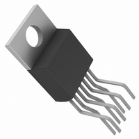
IC AMP C-FEEDBACK 1.1A TO-220-7
Manufacturer
Linear Technology
Datasheet
1.LT1210CT7PBF.pdf
(16 pages)
Specifications of LT1210CT7
Amplifier Type
Current Feedback
Number Of Circuits
1
Slew Rate
90 V/µs
-3db Bandwidth
55MHz
Current - Input Bias
10µA
Voltage - Input Offset
3000µV
Current - Supply
35mA
Current - Output / Channel
2A
Voltage - Supply, Single/dual (±)
10 V ~ 30 V, ±5 V ~ 15 V
Operating Temperature
0°C ~ 70°C
Mounting Type
Through Hole
Package / Case
TO-220-7 (Bent and Staggered Leads)
Lead Free Status / RoHS Status
Contains lead / RoHS non-compliant
Output Type
-
Gain Bandwidth Product
-
Available stocks
Company
Part Number
Manufacturer
Quantity
Price

Company:
Part Number:
LT1210CT7
Manufacturer:
XI;
Quantity:
5 510
Part Number:
LT1210CT7
Manufacturer:
LT
Quantity:
20 000
Part Number:
LT1210CT7#06PBF
Manufacturer:
LINEAR/凌特
Quantity:
20 000
Part Number:
LT1210CT7#37PBF
Manufacturer:
LINEAR/凌特
Quantity:
20 000
Part Number:
LT1210CT7#44PBF
Manufacturer:
LINEAR/凌特
Quantity:
20 000
Company:
Part Number:
LT1210CT7#PBF
Manufacturer:
LINEAR
Quantity:
1 250
Part Number:
LT1210CT7#PBF
Manufacturer:
LINEAR/凌特
Quantity:
20 000


Power Supplies
The LT1210 will operate from single or split supplies from
±5V (10V total) to ±15V (30V total). It is not necessary to
use equal value split supplies, however the offset voltage
and inverting input bias current will change. The offset
voltage changes about 500µV per volt of supply mis-
match. The inverting bias current can change as much as
5µA per volt of supply mismatch, though typically the
change is less than 0.5µA per volt.
Power Supply Bypassing
To obtain the maximum output and the minimum distor-
tion from the LT1210, the power supply rails should be
well bypassed. For example, with the output stage pouring
1A current peaks into the load, a 1Ω power supply imped-
ance will cause a droop of 1V, reducing the available
output swing by that amount. Surface mount tantalum and
ceramic capacitors make excellent low ESR bypass ele-
ments when placed close to the chip. For frequencies
above 100kHz, use 1µF and 100nF ceramic capacitors.
If significant power must be delivered below 100kHz,
capacitive reactance becomes the limiting factor. Larger
ceramic or tantalum capacitors, such as 4.7µF, are recom-
mended in place of the 1µF unit mentioned above.
Inadequate bypassing is evidenced by reduced output
swing and “distorted” clipping effects when the output is
driven to the rails. If this is observed, check the supply pins
of the device for ripple directly related to the output
waveform. Significant supply modulation indicates poor
bypassing.
Thermal Considerations
The LT1210 contains a thermal shutdown feature which
protects against excessive internal (junction) tempera-
ture. If the junction temperature of the device exceeds the
protection threshold, the device will begin cycling be-
tween normal operation and an off state. The cycling is not
harmful to the part. The thermal cycling occurs at a slow
rate, typically 10ms to several seconds, which depends on
the power dissipation and the thermal time constants of
the package and heat sinking. Raising the ambient tem-
perature until the device begins thermal shutdown gives a
good indication of how much margin there is in the
thermal design.
A
PPLICATI
O
U
S
I FOR ATIO
U
W
U
For surface mount devices heat sinking is accomplished
by using the heat spreading capabilities of the PC board
and its copper traces. Experiments have shown that the
heat spreading copper layer does not need to be electri-
cally connected to the tab of the device. The PCB material
can be very effective at transmitting heat between the pad
area attached to the tab of the device, and a ground or
power plane layer either inside or on the opposite side of
the board. Although the actual thermal resistance of the
PCB material is high, the length/area ratio of the thermal
resistance between the layer is small. Copper board stiff-
eners and plated through holes can also be used to spread
the heat generated by the device.
Tables 1 and 2 list thermal resistance for each package. For
the TO-220 package, thermal resistance is given for junc-
tion-to-case only since this package is usually mounted to
a heat sink. Measured values of thermal resistance for
several different board sizes and copper areas are listed for
each surface mount package. All measurements were
taken in still air on 3/32" FR-4 board with 2 oz copper. This
data can be used as a rough guideline in estimating
thermal resistance. The thermal resistance for each appli-
cation will be affected by thermal interactions with other
components as well as board size and shape.
Table 1. R Package, 7-Lead DD
2500 sq. mm 2500 sq. mm
1000 sq. mm 2500 sq. mm
125 sq. mm
*Tab of device attached to topside copper
Table 2. Fused 16-Lead SO Package
2500 sq. mm 2500 sq. mm 5000 sq. mm
1000 sq. mm 2500 sq. mm 3500 sq. mm
600 sq. mm
180 sq. mm
180 sq. mm
180 sq. mm
180 sq. mm
180 sq. mm
180 sq. mm
TOPSIDE*
TOPSIDE
COPPER AREA
COPPER AREA
2500 sq. mm
2500 sq. mm 3100 sq. mm
2500 sq. mm 2680 sq. mm
1000 sq. mm 1180 sq. mm
600 sq. mm
300 sq. mm
100 sq. mm
BACKSIDE
BACKSIDE
0 sq. mm
BOARD AREA (JUNCTION-TO-AMBIENT)
BOARD AREA (JUNCTION-TO-AMBIENT)
2500 sq. mm
2500 sq. mm
2500 sq. mm
780 sq. mm
480 sq. mm
280 sq. mm
180 sq. mm
THERMAL RESISTANCE
THERMAL RESISTANCE
25°C/W
27°C/W
35°C/W
40°C/W
46°C/W
48°C/W
49°C/W
56°C/W
58°C/W
59°C/W
60°C/W
61°C/W
LT1210
11
1210fa
Related parts for LT1210CT7
Image
Part Number
Description
Manufacturer
Datasheet
Request
R

Part Number:
Description:
1.1A/ 35MHz Current Feedback Amplifier
Manufacturer:
Linear Technology
Datasheet:
Part Number:
Description:
CD ROM LINEARVIEW DATASHEETS
Manufacturer:
Linear Technology

Part Number:
Description:
Standalone Linear Li-Ion Battery Charger with Thermal Regulation in ThinSOT
Manufacturer:
Linear Technology Corporation
Datasheet:
Part Number:
Description:
Low noise, high frequency, 8th order linear phase lowpass filter
Manufacturer:
Linear Technology Corporation
Datasheet:
Part Number:
Description:
Manufacturer:
Linear Technology Corporation
Datasheet:
Part Number:
Description:
Manufacturer:
Linear Technology Corporation
Datasheet:
Part Number:
Description:
Manufacturer:
Linear Technology Corporation
Datasheet:
Part Number:
Description:
Manufacturer:
Linear Technology Corporation
Datasheet:
Part Number:
Description:
Manufacturer:
Linear Technology Corporation
Datasheet:
Part Number:
Description:
Manufacturer:
Linear Technology Corporation
Datasheet:
Part Number:
Description:
Manufacturer:
Linear Technology Corporation
Datasheet:
Part Number:
Description:
Dual and Quad, JFET Input Precision High Speed Op Amps
Manufacturer:
Linear Technology Corporation
Datasheet:
Part Number:
Description:
Manufacturer:
Linear Technology Corporation
Datasheet:
Part Number:
Description:
1, 2, 6 and 8 Channel, 10-Bit Serial I/O Data Acquisition Systems
Manufacturer:
Linear Technology Corporation
Datasheet:
Part Number:
Description:
Manufacturer:
Linear Technology Corporation
Datasheet: