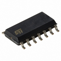
TL064ID STMicroelectronics, TL064ID Datasheet - Page 3

TL064ID
Manufacturer Part Number
TL064ID
Description
IC OPAMP JFET QUAD LO PWR 14SOIC
Manufacturer
STMicroelectronics
Datasheet
1.TL064CN.pdf
(14 pages)
Specifications of TL064ID
Amplifier Type
J-FET
Number Of Circuits
4
Slew Rate
3.5 V/µs
Gain Bandwidth Product
1MHz
Current - Input Bias
30pA
Voltage - Input Offset
3000µV
Current - Supply
200µA
Current - Output / Channel
20mA
Voltage - Supply, Single/dual (±)
6 V ~ 36 V, ±3 V ~ 18 V
Operating Temperature
-40°C ~ 105°C
Mounting Type
Surface Mount
Package / Case
14-SOIC (3.9mm Width), 14-SOL
Lead Free Status / RoHS Status
Lead free / RoHS Compliant
Output Type
-
-3db Bandwidth
-
Available stocks
Company
Part Number
Manufacturer
Quantity
Price
Company:
Part Number:
TL064ID
Manufacturer:
TEXAS
Quantity:
2 062
Part Number:
TL064ID
Manufacturer:
ST
Quantity:
20 000
Company:
Part Number:
TL064IDR
Manufacturer:
Texas Instruments
Quantity:
18 150
Part Number:
TL064IDR
Manufacturer:
TI/德州仪器
Quantity:
20 000
Part Number:
TL064IDR TI
Manufacturer:
TI/德州仪器
Quantity:
20 000
Part Number:
TL064IDRG4
Manufacturer:
TI/德州仪器
Quantity:
20 000
Company:
Part Number:
TL064IDT
Manufacturer:
TOSH
Quantity:
5 922
Part Number:
TL064IDT
Manufacturer:
ST
Quantity:
20 000
TL064
2
Table 1.
1. All voltage values, except differential voltage, are with respect to the zero reference level (ground) of the supply voltages
2. The magnitude of the input voltage must never exceed the magnitude of the supply voltage or 15 volts, whichever is less.
3. Differential voltages are the non-inverting input terminal with respect to the inverting input terminal.
4. Short-circuits can cause excessive heating and destructive dissipation.
5. Rth are typical values.
6. The output may be shorted to ground or to either supply. Temperature and/or supply voltages must be limited to ensure
7. Human body model: 100pF discharged through a 1.5kΩ resistor between two pins of the device, done for all couples of pin
8. Machine model: a 200pF cap is charged to the specified voltage, then discharged directly between two pins of the device
9. Charged device model: all pins plus package are charged together to the specified voltage and then discharged directly to
Table 2.
Symbol
Symbol
R
T
ESD
R
V
T
T
P
where the zero reference level is the midpoint between V
that the dissipation rating is not exceeded.
combinations with other pins floating.
with no external series resistor (internal resistor < 5Ω), done for all couples of pin combinations with other pins floating.
the ground.
V
V
oper
V
oper
CC
thja
thjc
stg
tot
CC
id
i
Supply voltage
Input voltage
Differential input voltage
Power dissipation
Thermal resistance junction to
ambient
Thermal resistance junction to
case
Output short-circuit duration
Operating free-air temperature range
Storage temperature range
HBM: human body model
MM: machine model
CDM: charged device model
Supply voltage range
Operating free-air temperature range
SO-14
DIP14
SO-14
DIP14
Absolute maximum ratings and operating conditions
Absolute maximum ratings
Operating conditions
(4) (5)
(4) (5)
(2)
Parameter
Parameter
(1)
(8)
(3)
(7)
(9)
(6)
TL064M, AM, BM TL064I, AI, BI
TL064M, AM, BM TL064I, AI, BI
Absolute maximum ratings and operating conditions
CC
-55 to +125
-55 to +125
+
and V
CC
-
.
-40 to +105
-40 to +105
-65 to +150
6 to 36
Infinite
Value
1500
±18
±15
±30
680
105
900
200
80
31
33
TL064C, AC, BC
TL064C, AC, BC
0 to +70
0 to +70
°C/W
°C/W
Unit
Unit
mW
°C
°C
°C
V
V
V
V
V
3/14


