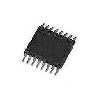
TSV6295AIPT STMicroelectronics, TSV6295AIPT Datasheet - Page 13

TSV6295AIPT
Manufacturer Part Number
TSV6295AIPT
Description
IC OP AMP MICROPWR WIDE 16TSSOP
Manufacturer
STMicroelectronics
Datasheet
1.TSV6294IPT.pdf
(25 pages)
Specifications of TSV6295AIPT
Amplifier Type
General Purpose
Number Of Circuits
4
Output Type
Rail-to-Rail
Slew Rate
0.5 V/µs
Gain Bandwidth Product
1.3MHz
Current - Input Bias
1pA
Voltage - Input Offset
800µV
Current - Supply
29µA
Current - Output / Channel
74mA
Voltage - Supply, Single/dual (±)
1.5 V ~ 5.5 V
Operating Temperature
-40°C ~ 125°C
Mounting Type
Surface Mount
Package / Case
16-TSSOP
Number Of Channels
Quad
Common Mode Rejection Ratio (min)
51 dB
Input Voltage Range (max)
5.5 V
Input Voltage Range (min)
1.5 V
Input Offset Voltage
2 mV
Input Bias Current (max)
100 pA
Supply Current
33 uA
Maximum Operating Temperature
+ 125 C
Minimum Operating Temperature
- 40 C
Mounting Style
SMD/SMT
Operating Temperature Range
- 40 C to + 125 C
Supply Voltage (max)
5.5 V
Supply Voltage (min)
1.5 V
Thd Plus Noise
0.03 %
Voltage Gain Db
95 dB
Lead Free Status / RoHS Status
Lead free / RoHS Compliant
-3db Bandwidth
-
Lead Free Status / Rohs Status
Lead free / RoHS Compliant
Other names
497-10460-2
Available stocks
Company
Part Number
Manufacturer
Quantity
Price
Company:
Part Number:
TSV6295AIPT
Manufacturer:
STMicroelectronics
Quantity:
2 000
TSV629x, TSV629xA
4
4.1
4.2
4.3
Figure 19. Input offset voltage vs input
Application information
Operating voltages
The TSV629x can operate from 1.5 to 5.5 V. The devices’ parameters are fully specified for
1.8, 3.3 and 5 V power supplies. However, the parameters are very stable in the full V
range and several characterization curves show the TSV629x characteristics at 1.5 V.
Additionally, the main specifications are guaranteed in extended temperature ranges from
-40° C to +125° C.
Rail-to-rail input
The TSV629x are built with two complementary PMOS and NMOS input differential pairs.
The devices have a rail-to-rail input, and the input common mode range is extended from
V
In the transition region, the performance of CMR, SVR, V
THD is slightly degraded.
The devices are guaranteed without phase reversal.
Rail-to-rail output
The operational amplifiers’ output level can go close to the rails: 35 mV maximum above and
below the rail when connected to a 10 kΩ resistive load to V
common mode at V
CC-
- 0.1 V to V
CC+
+ 0.1 V. The transition between the two pairs appears at V
CC
= 1.5 V
Doc ID 16882 Rev 2
Figure 20. Input offset voltage vs input
common mode at V
io
(Figure 19
CC
/2.
Application information
and
CC
Figure
= 5 V
CC+
20) and
- 0.7 V.
CC
13/25


