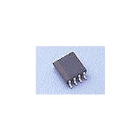
TSV612AIST STMicroelectronics, TSV612AIST Datasheet

TSV612AIST
Specifications of TSV612AIST
Available stocks
Related parts for TSV612AIST
TSV612AIST Summary of contents
Page 1
TSV611, TSV611A, TSV612, TSV612A Features ■ Rail-to-rail input and output ■ Low power consumption: 10 µA typ ■ Low supply voltage: 1.5 to 5.5 V ■ Gain bandwidth product: 120 kHz typ ■ Unity gain stable ■ ...
Page 2
Absolute maximum ratings and operating conditions 1 Absolute maximum ratings and operating conditions Table 1. Absolute maximum ratings Symbol V Supply voltage CC V Differential input voltage id V Input voltage in T Storage temperature stg Thermal resistance junction to ...
Page 3
TSV611, TSV611A, TSV612, TSV612A 2 Electrical characteristics Table 3. Electrical characteristics at V with V (unless otherwise specified) Symbol DC performance V Offset voltage io DV Input offset voltage drift io Input offset current out ...
Page 4
Electrical characteristics Table 3. Electrical characteristics at V with V (unless otherwise specified) (continued) Symbol Equivalent input noise e n voltage Total harmonic distortion + THD+N noise 1. Guaranteed by design. 4/19 CC /2, ...
Page 5
TSV611, TSV611A, TSV612, TSV612A Table 4. V CC+ R connected Symbol DC performance V Offset voltage io DV Input offset voltage drift io I Input offset current io I Input bias current ib Common mode rejection CMR ...
Page 6
Electrical characteristics Table 5. V CC+ (unless otherwise specified) Symbol DC performance V Offset voltage io DV Input offset voltage drift io I Input offset current io I Input bias current ib Common mode rejection CMR ratio 20 log (ΔV ...
Page 7
TSV611, TSV611A, TSV612, TSV612A Table 5. V CC+ (unless otherwise specified) (continued) Symbol Equivalent input noise e n voltage Total harmonic distortion + THD+N noise 1. Guaranteed by design. Figure 1. Supply current vs. supply voltage ...
Page 8
Electrical characteristics Figure 5. Voltage gain and phase vs. frequency Figure 7. Positive slew rate vs. time 100 pF, R Load T=− 40°C T=25°C V =1.5V =10k Load Time (µs) Figure ...
Page 9
TSV611, TSV611A, TSV612, TSV612A Figure 11. Slew rate vs. supply voltage Figure 13. Distortion + noise vs. frequency 1 Vcc=1.5V Ω Rl=10k 0.1 Vcc=1.5V Ω Rl=100k 0.01 10 100 Figure 15. Voltage gain and phase vs. frequency ...
Page 10
Application information 3 Application information 3.1 Operating voltages The TSV61x can operate from 1.5 to 5.5 V. Their parameters are fully specified for 1.8, 3.3 and 5 V power supplies. However, the parameters are very stable in the full V ...
Page 11
... Macromodel An accurate macromodel of the TSV61x is available on STMicroelectronics’ web site at www.st.com. This model is a trade-off between accuracy and complexity (that is, time simulation) of the TSV61x operational amplifiers. It emulates the nominal performances of a typical device within the specified operating conditions mentioned in the datasheet. It also helps to validate a design approach and to select the right operational amplifier, but it does not replace on-board measurements ...
Page 12
Package information 4 Package information In order to meet environmental requirements, ST offers these devices in different grades of ® ECOPACK packages, depending on their level of environmental compliance. ECOPACK specifications, grade definitions and product status are available at: www.st.com. ...
Page 13
TSV611, TSV611A, TSV612, TSV612A 4.1 SOT23-5 package information Figure 20. SOT23-5 package mechanical drawing Table 6. SOT23-5 package mechanical data Ref degrees Dimensions Millimeters Min. Typ. Max. ...
Page 14
Package information 4.2 SC70-5 (SOT323-5) package information Figure 21. SC70-5 (SOT323-5) package mechanical drawing Table 7. SC70-5 (SOT323-5) package mechanical data Ref < 14/19 DIMENSIONS IN MM GAUGE PLANE ...
Page 15
TSV611, TSV611A, TSV612, TSV612A 4.3 SO-8 package information Figure 22. SO-8 package mechanical drawing Table 8. SO-8 package mechanical data Ref ccc Dimensions Millimeters Min. Typ. Max. ...
Page 16
Package information 4.4 MiniSO-8 package information Figure 23. MiniSO-8 package mechanical drawing Table 9. MiniSO-8 package mechanical data Ref ccc 16/19 Dimensions Millimeters Min. Typ. Max. 1.1 ...
Page 17
... TSV611, TSV611A, TSV612, TSV612A 5 Ordering information Table 10. Order codes Order code TSV611ILT TSV611AILT TSV611ICT TSV611AICT TSV612ID/DT TSV612AID/DT TSV612IST TSV612AIST Temperature Package range SOT23-5 SC70-5 -40° 85° C SO-8 MiniSO-8 Doc ID 15768 Rev 2 Ordering information Packing Marking K12 K11 Tape & reel K12 ...
Page 18
Revision history 6 Revision history Table 11. Document revision history Date 28-May-2009 18-Jan-2010 18/19 Revision 1 Initial release. Full datasheet for product now in production. 2 Added Figure 1 to Figure Doc ID 15768 Rev 2 TSV611, TSV611A, TSV612, TSV612A ...
Page 19
... TSV611, TSV611A, TSV612, TSV612A Information in this document is provided solely in connection with ST products. STMicroelectronics NV and its subsidiaries (“ST”) reserve the right to make changes, corrections, modifications or improvements, to this document, and the products and services described herein at any time, without notice. All ST products are sold pursuant to ST’s terms and conditions of sale. ...


