TS613IDT STMicroelectronics, TS613IDT Datasheet
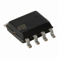
IC AMP DUAL WIDE BAND OP 8 SOIC

TS613IDT

Manufacturer Part Number
TS613IDT
Description
IC AMP DUAL WIDE BAND OP 8 SOIC
Manufacturer
STMicroelectronics
Datasheet

Specifications of TS613IDT

Amplifier Type
Voltage Feedback
Number Of Circuits
2
Slew Rate
40 V/µs
Gain Bandwidth Product
130MHz
Current - Input Bias
5µA
Voltage - Input Offset
1000µV
Current - Supply
11mA
Current - Output / Channel
320mA
Voltage - Supply, Single/dual (±)
5 V ~ 12 V, ±2.5 V ~ 6 V
Operating Temperature
-40°C ~ 85°C
Mounting Type
Surface Mount
Package / Case
8-SOIC (3.9mm Width)
Number Of Channels
2
Voltage Gain Db
80.83 dB
Common Mode Rejection Ratio (min)
90 dB
Input Offset Voltage
6 mV
Supply Current
22 mA
Maximum Power Dissipation
2000 mW
Maximum Operating Temperature
+ 85 C
Mounting Style
SMD/SMT
Maximum Dual Supply Voltage
+/- 6 V
Minimum Operating Temperature
- 40 C
Power Supply Requirement
Single/Dual
Pin Count
8
Lead Free Status / RoHS Status
Lead free / RoHS Compliant
Output Type
-
-3db Bandwidth
-
Lead Free Status / Rohs Status
 Details
Other names
497-2302-2

Available stocks

Company
Part Number
Manufacturer
Quantity
Price
Part Number:
TS613IDT
Manufacturer:
ST
0
Part Number:
TS613IDT
Manufacturer:
ST
Quantity:
20 000
DESCRIPTION
The TS613 is a dual operational amplifier featur-
ing a high output current (200mA min.), large
gain-bandwidth product (130MHz) and capable of
driving a 25
This device is particularly intended for applications
where multiple carriers must be amplified simulta-
neously with very low intermodulation products.
The TS613 is housed in a SO8 plastic package
and a SO8 Exposed-Pad plastic package.
APPLICATION
ORDER CODE
D = Small Outline Package (SO) - also available in Tape & Reel (DT)
DW = Small Outline Package inExposed-Pad (SO) - also available in
December 2002
TS613ID
TS613IDW
6V power supply.
Number
LOW NOISE : 3nV/ Hz, 1.2pA/ Hz
HIGH OUTPUT CURRENT : 200mA
VERY LOW HARMONIC AND INTERMODU-
LATION DISTORTION
HIGH SLEW RATE : 40V/ s
SPECIFIED FOR 25 LOAD
UPSTREAM line driver for Asymmetric Digital
Subscriber Line (ADSL) (NT).
Part
Tape & Reel (DWT)
load with a 160mA output current at
Temperature
-40, +85°C
-40, +85°C
Range
DUAL WIDE BAND OPERATIONAL AMPLIFIER
D
Package
DW
WITH HIGH OUTPUT CURRENT
PIN CONNECTIONS (top view)
Non Inverting Input1
This pad can be connected to a (-Vcc) copper area on the PCB
Inverting Input1
Inverting Input1
Output1
Output1
Cross Section View Showing Exposed-Pad
VCC -
VCC -
(Plastic Micropackage)
1
1
2
2
3
3
4
4
SO8 Exposed-Pad
+
+
+
+
_
_
_
_
SO8
D
DW
_
_
_
+
+
+
8
8
7
7
6
6
5
5
VCC +
VCC +
Non Inverting Input2
Inverting Input2
Inverting Input2
Output2
Output2
TS613
1/10

Related parts for TS613IDT

TS613IDT Summary of contents

Page 1

DUAL WIDE BAND OPERATIONAL AMPLIFIER LOW NOISE : 3nV/ Hz, 1.2pA/ Hz HIGH OUTPUT CURRENT : 200mA VERY LOW HARMONIC AND INTERMODU- LATION DISTORTION HIGH SLEW RATE : 40V/ s SPECIFIED FOR 25 LOAD DESCRIPTION The TS613 is a dual ...

Page 2

TS613 ABSOLUTE MAXIMUM RATINGS Symbol 1) V Supply voltage CC V Differential Input Voltage Input Voltage Range in T Operating Free Air Temperature Range oper T Storage Temperature std T Maximum Junction Temperature j Output Short Circuit ...

Page 3

ELECTRICAL CHARACTERISTICS Symbol Parameter DC PERFORMANCE V Input Offset Voltage io V Differential Input Offset Voltage io I Input Offset Current io I Input Bias Current ib CMR Common Mode Rejection Ratio SVR Supply Voltage Rejection Ratio I Total Supply ...

Page 4

TS613 THERMAL INFORMATION The TS613 is housed in an Exposed-Pad plastic package. As described on the figures below, this package uses a leadframe upon which the dice is mounted. This leadframe is exposed as a thermal pad on the underside ...

Page 5

Closed Loop Gain and Phase vs. Frequency ± Gain=+2, Vcc= 6V, RL=25 10 Gain 0 Phase -10 -20 -30 10kHz 100kHz 1MHz 10MHz Frequency Closed Loop Gain and Phase vs. Frequency ± Gain=+11, Vcc= 6V, RL=25 30 Gain 20 10 ...

Page 6

TYPICAL APPLICATION : TS613 AS DRIVER A SINGLE SUPPLY IMPLEMENTATION WITH PASSIVE ADSL CONCEPT Asymmetric Digital Subscriber Line (ADSL new modem technology, which converts the exist- ing twisted-pair telephone lines into access paths for multimedia and high speed ...

Page 7

F capacitance provides a path for low frequen- cies, the 10nF capacitance provides a path for high end of the spectrum. In differential mode the TS613 is able to deliver a typical amplitude signal of 18V peak to peak. ...

Page 8

TS613 By identification of both equations (2) and (3), the synthesized impedance is, with Rs1=Rs2=Rs: Rs ---------------- - ------ - – R3 Figure 5 : Equivalent schematic the syn- thesized impedance Iout ...

Page 9

PACKAGE MECHANICAL DATA 8 PINS - PLASTIC MICROPACKAGE (SO) Dim. Min 0 0.65 b 0.35 b1 0. 4 3 Millimeters Typ. Max. 1.75 ...

Page 10

... No license is granted by implication or otherwise under any patent or patent rights of STMicroelectronics. Specifications mentioned in this publication are subject to change without notice. This publication supersedes and replaces all information previously supplied ...

Related keywords