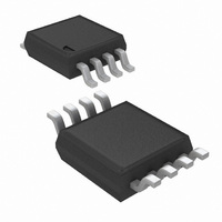
LMP8602MMX/NOPB National Semiconductor, LMP8602MMX/NOPB Datasheet - Page 2

LMP8602MMX/NOPB
Manufacturer Part Number
LMP8602MMX/NOPB
Description
IC AMP CURRENT SENSE 60V 8-MSOP
Manufacturer
National Semiconductor
Series
LMP®r
Datasheet
1.LMP8602MMENOPB.pdf
(24 pages)
Specifications of LMP8602MMX/NOPB
Amplifier Type
Current Sense
Number Of Circuits
1
Slew Rate
0.83 V/µs
Gain Bandwidth Product
60kHz
Current - Input Bias
0.04pA
Voltage - Input Offset
150µV
Current - Supply
1.1mA
Current - Output / Channel
48mA
Voltage - Supply, Single/dual (±)
3 V ~ 5.5 V
Operating Temperature
-40°C ~ 125°C
Mounting Type
Surface Mount
Package / Case
8-MSOP, Micro8™, 8-uMAX, 8-uSOP,
Lead Free Status / RoHS Status
Lead free / RoHS Compliant
Output Type
-
-3db Bandwidth
-
Other names
LMP8602MMX
www.national.com
Overall Performance (From -IN (pin 1) and +IN (pin 8) to OUT (pin 5) with pins A1 (pin 3) and A2 (pin 4) connected)
I
A
SR
BW
V
TCV
e
PSRR
Preamplifier (From input pins -IN (pin 1) and +IN (pin 8) to A1 (pin 3))
R
R
V
DC CMRR DC Common Mode Rejection Ratio
AC CMRR
CMVR
K1
R
TCR
A1 V
S
n
Symbol
V
OS
OS
CM
DM
F-INT
Absolute Maximum Ratings
If Military/Aerospace specified devices are required,
please contact the National Semiconductor Sales Office/
Distributors for availability and specifications.
3.3V Electrical Characteristics
Unless otherwise specified, all limits guaranteed at T
7) is grounded, 10nF between V
ESD Tolerance
Supply Voltage (V
Continuous Input Voltage (−IN
and +IN)
Maximum Voltage at A1, A2,
OFFSET and OUT Pins
OS
F-INT
OUT
Human Body
Machine Model
Charge Device Model
Transient (400 ms)
For input pins only
For all other pins
Supply Current
Total Gain
Gain Drift
Slew Rate
Bandwidth
Input Offset Voltage
Input Offset Voltage Drift
Input Referred Voltage Noise
Power Supply Rejection Ratio
Mid−scale Offset Scaling Accuracy
Input Impedance Common Mode
Input Impedance Differential Mode
Input Offset Voltage
AC Common Mode Rejection Ratio
(Note
Input Common Mode Voltage Range
Gain
Output Impedance Filter Resistor
Output Impedance Filter Resistor Drift
A1 Output Voltage Swing
(Note
(Note
10)
6)
(Note
S
(Note
(Note
- GND)
15)
4)
Parameter
15)
8)
S
and GND. Boldface limits apply at the temperature extremes.
(Note
9)
V
−22V to 60V
−25V to 65V
S
(Note
GND -0.3V
+0.3V and
±4000V
±2000V
1000V
A
(Note
LMP8602
LMP8603
−40°C
V
V
−40°C
0.1 Hz − 10 Hz, 6 Sigma
Spectral Density, 1 kHz
DC, 3.0V
LMP8602
LMP8603
−4V
−4V
V
−2V
f = 1 kHz
f = 10 kHz
for 80 dB CMRR
V
V
1)
200V
6.0V
= 25°C, V
IN
CM
CM
OL
OH
= ±0.165V
= V
≤
≤
= V
≤
2)
V
V
V
≤
≤
S
S
CM
CM
CM
T
T
/ 2
≤
/ 2
2
A
A
S
≤
≤
≤
V
Conditions
≤
≤
= 3.3V, GND = 0V, −4V
S
27V
27V
24V
125°C
125°C
Operating Ratings
≤
Storage Temperature Range
Junction Temperature
Mounting Temperature
Supply Voltage (V
Offset Voltage (Pin 7 )
Temperature Range
Packaged devices
Package Thermal Resistance
3.6V, V
Infrared or Convection (20 sec)
Wave Soldering Lead (10 sec)
8-Pin SOIC (θ
8-Pin MSOP (θ
Input Referred
Input Referred
R
L
CM
=
∞
= V
S
JA
/2
JA
S
)
)
– GND)
≤
(Note
(Note
(Note
V
49.75
99.5
9.95
Min
250
500
0.4
3.2
CM
50
70
86
80
−4
99
3)
≤
7)
3)
27V, and R
(Note
(Note
(Note
±0.25
±0.45
±0.15
−2.7
0.15
16.4
10.0
3.25
Typ
100
830
295
590
100
0.7
50
60
86
96
94
85
±5
1
2
2
3)
1)
5)
−40°C to +125°C
L
−65°C to 150°C
(Note
=
±0.248
50.25
100.5
±0.33
10.05
Max
±1.5
±20
±10
350
700
101
±50
∞
1.3
±1
±1
±1
27
10
3.0V to 5.5V
, Offset (Pin
190°C/W
203°C/W
7)
0 to V
150°C
235°C
260°C
ppm/°C
nV/
ppm/°C
μV/°C
Units
μV
V/μs
kHz
mA
V/V
mV
mV
mV
mV
V/V
mV
dB
kΩ
kΩ
dB
dB
kΩ
%
%
V
V
√
S
P-P
Hz


