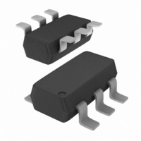
NCV2002SN2T1G ON Semiconductor, NCV2002SN2T1G Datasheet - Page 11

NCV2002SN2T1G
Manufacturer Part Number
NCV2002SN2T1G
Description
IC OPAMP R-R 0.9V 1A 6-TSOP
Manufacturer
ON Semiconductor
Datasheet
1.NCS2002SN1T1G.pdf
(16 pages)
Specifications of NCV2002SN2T1G
Amplifier Type
General Purpose
Number Of Circuits
1
Output Type
Rail-to-Rail
Slew Rate
1.3 V/µs
Gain Bandwidth Product
900kHz
Current - Input Bias
10pA
Voltage - Input Offset
500µV
Current - Supply
820µA
Current - Output / Channel
128mA
Voltage - Supply, Single/dual (±)
0.9 V ~ 7 V, ±0.45 V ~ 3.5 V
Operating Temperature
-40°C ~ 125°C
Mounting Type
Surface Mount
Package / Case
SC-74-6
Number Of Channels
1
Voltage Gain Db
92.04 dB
Common Mode Rejection Ratio (min)
60 dB
Input Voltage Range (max)
Positive Rail
Input Voltage Range (min)
Negative Rail
Input Offset Voltage
6 mV
Operating Supply Voltage
7 V
Supply Current
2 uA
Maximum Power Dissipation
340 mW
Maximum Operating Temperature
+ 125 C
Mounting Style
SMD/SMT
Maximum Dual Supply Voltage
+/- 3.5 V
Minimum Operating Temperature
- 40 C
Lead Free Status / RoHS Status
Lead free / RoHS Compliant
-3db Bandwidth
-
Lead Free Status / Rohs Status
Details
Other names
NCV2002SN2T1G
NCV2002SN2T1GOSTR
NCV2002SN2T1GOSTR
Available stocks
Company
Part Number
Manufacturer
Quantity
Price
Part Number:
NCV2002SN2T1G
Manufacturer:
ON/安森美
Quantity:
20 000
Output
channel devices connected to provide rail−to−rail output
drive. With a 2.0 k load, the output can swing within 50 mV
of either rail. It is also capable of supplying over 75 mA
when powered from 5.0 V and 1.0 mA when powered from
0.9 V.
can directly drive capacitive loads in excess of 820 pF at
room temperature without oscillating but with significantly
reduced phase margin. The unity gain follower
configuration exhibits the highest bandwidth and is most
prone to oscillations when driving a high value capacitive
load. The capacitive load in combination with the
amplifier’s output impedance, creates a phase lag that can
result in an under−damped pulse response or a continuous
oscillation. Figure 35 shows the effect of driving a large
capacitive load in a voltage follower type of setup. When
driving capacitive loads exceeding 820 pF, it is
recommended to place a low value isolation resistor
between the output of the op amp and the load, as shown in
Figure 34. The series resistor isolates the capacitive load
from the output and enhances the phase margin. Refer to
Figure 36. Larger values of R will result in a cleaner output
waveform but excessively large values will degrade the
The output stage consists of complementary P and N
When connected as a unity gain follower, the NCS2002
http://onsemi.com
11
large signal rise and fall time and reduce the output
amplitude. Depending upon the capacitor characteristics,
the isolation resistor value will typically be between 50 to
500 W. The output drive capability for resistive and
capacitive loads is shown in Figures 2, 3, and 23.
temperature and low supply voltage.
Enable Pin
device. if the enable pin is pulled below the input disable
threshold voltage (V
disabled. Once the enable pin is taken above the threshold
voltage (V
event the enable pin is not connected, the amplifier will
remain on by default
Note that the lowest phase margin is observed at cold
The enable pin allows the user to externally control the
Figure 34. Capacitance Load Isolation
Input
EN
= 60% V
Isolation resistor R = 50 to 500
+
−
EN
CC
), the amplifier will turn on. In the
< 45% V
R
CC
), the amplifier is
Output
C
L


