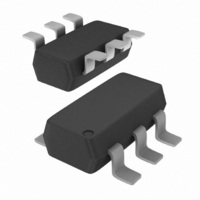
NCV2002SN2T1G ON Semiconductor, NCV2002SN2T1G Datasheet - Page 4

NCV2002SN2T1G
Manufacturer Part Number
NCV2002SN2T1G
Description
IC OPAMP R-R 0.9V 1A 6-TSOP
Manufacturer
ON Semiconductor
Datasheet
1.NCS2002SN1T1G.pdf
(16 pages)
Specifications of NCV2002SN2T1G
Amplifier Type
General Purpose
Number Of Circuits
1
Output Type
Rail-to-Rail
Slew Rate
1.3 V/µs
Gain Bandwidth Product
900kHz
Current - Input Bias
10pA
Voltage - Input Offset
500µV
Current - Supply
820µA
Current - Output / Channel
128mA
Voltage - Supply, Single/dual (±)
0.9 V ~ 7 V, ±0.45 V ~ 3.5 V
Operating Temperature
-40°C ~ 125°C
Mounting Type
Surface Mount
Package / Case
SC-74-6
Number Of Channels
1
Voltage Gain Db
92.04 dB
Common Mode Rejection Ratio (min)
60 dB
Input Voltage Range (max)
Positive Rail
Input Voltage Range (min)
Negative Rail
Input Offset Voltage
6 mV
Operating Supply Voltage
7 V
Supply Current
2 uA
Maximum Power Dissipation
340 mW
Maximum Operating Temperature
+ 125 C
Mounting Style
SMD/SMT
Maximum Dual Supply Voltage
+/- 3.5 V
Minimum Operating Temperature
- 40 C
Lead Free Status / RoHS Status
Lead free / RoHS Compliant
-3db Bandwidth
-
Lead Free Status / Rohs Status
Details
Other names
NCV2002SN2T1G
NCV2002SN2T1GOSTR
NCV2002SN2T1GOSTR
Available stocks
Company
Part Number
Manufacturer
Quantity
Price
Part Number:
NCV2002SN2T1G
Manufacturer:
ON/安森美
Quantity:
20 000
AC ELECTRICAL CHARACTERISTICS
Equivalent Input Noise Voltage (f = 1.0 kHz)
Time Delay for Device to Turn On (R
Time Delay for Device to Turn Off (R
Differential Input Resistance (V
Differential Input Capacitance (V
Gain Bandwidth Product (f = 100 kHz)
Gain Margin (R
Phase Margin (R
Power Bandwidth (V
Total Harmonic Distortion (V
Slew Rate (V
V
V
V
f = 1.0 kHz
f = 10 kHz
Positive Slope
Negative Slope
CC
CC
CC
= 0.45 V, V
= 1.5 V, V
= 2.5 V, V
S
= $2.5 V, V
L
L
= 10 k, C
EE
EE
= 10 k, C
EE
O
= −1.5 V
= −2.5 V
= −0.45 V
= 4.0 V
L
O
= 5.0 pf)
L
O
= −2.0 V to 2.0 V, R
= 5.0 pf)
PP
= 4.0 V
CM
, R
CM
= 0 V)
L
= 0 V)
L
L
= 2.0 k, THD = 1.0 %, A
Rating
PP
= 10 k)
= 10 k)
, R
L
= 2.0 k, A
(V
CC
L
= 2.0 k, A
= 2.5 V, V
V
= 1.0)
http://onsemi.com
V
V
EE
= 1.0)
= 1.0)
= −2.5 V, V
4
CM
= V
O
= 0 V, R
Symbol
GBW
BW
THD
Am
fm
R
C
SR
t
t
e
on
off
in
in
n
L
P
to GND, T
0.85
0.85
Min
0.6
−
−
−
−
−
−
−
−
−
−
−
−
A
= 25°C, unless otherwise noted)
0.008
>1.0
0.08
Typ
100
3.0
0.8
0.8
0.9
6.5
1.2
1.3
5.5
2.5
60
80
Max
7.5
3.0
−
−
−
−
−
−
−
−
−
−
−
−
−
nV/ Hz
tera W
MHz
Unit
V/ms
Deg
kHz
dB
ms
ms
%
pf


