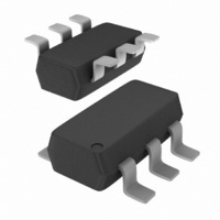
NCV2002SN2T1G ON Semiconductor, NCV2002SN2T1G Datasheet - Page 13

NCV2002SN2T1G
Manufacturer Part Number
NCV2002SN2T1G
Description
IC OPAMP R-R 0.9V 1A 6-TSOP
Manufacturer
ON Semiconductor
Datasheet
1.NCS2002SN1T1G.pdf
(16 pages)
Specifications of NCV2002SN2T1G
Amplifier Type
General Purpose
Number Of Circuits
1
Output Type
Rail-to-Rail
Slew Rate
1.3 V/µs
Gain Bandwidth Product
900kHz
Current - Input Bias
10pA
Voltage - Input Offset
500µV
Current - Supply
820µA
Current - Output / Channel
128mA
Voltage - Supply, Single/dual (±)
0.9 V ~ 7 V, ±0.45 V ~ 3.5 V
Operating Temperature
-40°C ~ 125°C
Mounting Type
Surface Mount
Package / Case
SC-74-6
Number Of Channels
1
Voltage Gain Db
92.04 dB
Common Mode Rejection Ratio (min)
60 dB
Input Voltage Range (max)
Positive Rail
Input Voltage Range (min)
Negative Rail
Input Offset Voltage
6 mV
Operating Supply Voltage
7 V
Supply Current
2 uA
Maximum Power Dissipation
340 mW
Maximum Operating Temperature
+ 125 C
Mounting Style
SMD/SMT
Maximum Dual Supply Voltage
+/- 3.5 V
Minimum Operating Temperature
- 40 C
Lead Free Status / RoHS Status
Lead free / RoHS Compliant
-3db Bandwidth
-
Lead Free Status / Rohs Status
Details
Other names
NCV2002SN2T1G
NCV2002SN2T1GOSTR
NCV2002SN2T1GOSTR
Available stocks
Company
Part Number
Manufacturer
Quantity
Price
Part Number:
NCV2002SN2T1G
Manufacturer:
ON/安森美
Quantity:
20 000
0.9 V
V
CC
1.0 nF
470 k
1.0 nF
470 k
R
R
C
C
1a
1a
T
T
470 k
R
1b
1.0 M
R
470 k
cww
cw
1b
470 k
−
+
0.9 V
R
10 k
10 k
470 k
T
−
+
R
V
2
CC
470 k
R
Figure 38. Variable Duty Cycle Pulse Generator
2
1N4148
1N4148
Figure 37. 0.9 V Square Wave Oscillator
D
D
1
2
f
O
http://onsemi.com
= 1.5 kHz
f
O
The timing capacitor C
through diode D
signal can be programmed by adjusting the value of the trimpot. The ca-
pacitor voltage will oscillate between 1/3 and 2/3 of V
resistors at the non−inverting input are of equal value.
Timing Capacitor
Timing Capacitor
13
Output Voltage
Output Voltage
Timing Capacitor
Output Voltage
Voltage
Voltage
The non−inverting input threshold levels are set so that
the capacitor voltage oscillates between 1/3 and 2/3 of
V
equal value. The following formula can be used to
approximate the output frequency.
CC
. This requires the resistors R
1
Voltage
, allowing a variable duty cycle. The pulse width of the
0.67 V
0.33 V
0.67 V
0.33 V
T
will charge through diode D
V
V
0.33 V
0.67 V
CC
CC
CC
CC
CC
CC
f
O
0
0
Counter−Clock−wise, High Duty Cycle
+
V
CC
CC
CC
1.39 R
0
Clock−wise, Low Duty Cycle
1
T
1a
C
T
, R
1b
and R
2
CC
and discharge
, since all the
2
to be of


