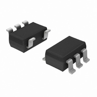
SA57000-30D,115 NXP Semiconductors, SA57000-30D,115 Datasheet - Page 8

SA57000-30D,115
Manufacturer Part Number
SA57000-30D,115
Description
IC LDO REG CAPFREE 150MA SOT23-5
Manufacturer
NXP Semiconductors
Series
CapFREE™r
Datasheet
1.SA57000-30D115.pdf
(15 pages)
Specifications of SA57000-30D,115
Package / Case
SOT-23-5, SC-74A, SOT-25
Regulator Topology
Positive Fixed
Voltage - Output
3V
Voltage - Input
Up to 6.5V
Voltage - Dropout (typical)
0.165V @ 150mA
Number Of Regulators
1
Current - Output
150mA
Current - Limit (min)
160mA
Operating Temperature
-40°C ~ 85°C
Mounting Type
Surface Mount
Number Of Outputs
1
Polarity
Positive
Input Voltage Max
6.5 V
Output Voltage
3 V
Output Type
Fixed
Dropout Voltage (max)
0.12 V at 50 mA
Output Current
150 mA
Line Regulation
0.1 % / V
Load Regulation
0.02 % / mA
Voltage Regulation Accuracy
1 %
Maximum Power Dissipation
0.637 W
Maximum Operating Temperature
+ 85 C
Mounting Style
SMD/SMT
Minimum Operating Temperature
- 40 C
Reference Voltage
1.23 V
Lead Free Status / RoHS Status
Lead free / RoHS Compliant
Lead Free Status / RoHS Status
Lead free / RoHS Compliant, Lead free / RoHS Compliant
Other names
568-3306-2
935269651115
SA57000-30D-G
935269651115
SA57000-30D-G
Philips Semiconductors
TECHNICAL DESCRIPTION
General discussion
The SA57000-XX is a low dropout, low-quiescent current linear
regulator designed primarily for battery-powered applications and
stabilizes with or without input/output capacitors. The device delivers
up to 150 mA and is available with preset output voltages of 2.5 V,
2.8 V, 2.9 V, 3.0 V, 3.1 V, 3.3 V, and 3.6 V for both SOT 23-5 and
WL-CSP packages.
The 1.23 band-gap reference is connected to the error amplifier’s
inverting input. The error amplifier compares this reference with the
feedback voltage and amplifies the difference. If the feedback
voltage is lower than the reference voltage, the pass-transistor gate
is pulled lower, which allows more current to pass to the output. The
output voltage is fed back through an internal resistor voltage divider
connected to the V
Band-gap
The band-gap circuitry generates a temperature independent
voltage by properly adding two voltages with negative and positive
temperature coefficient. The band-gap voltage is typically 1.23 volts
with a temperature variation of 5 mV over the temperature range
from –40 C to +125 C.
Low-pass filter
Low-pass filter is basically an RC filter with a low cut-off frequency.
No external capacitor is used. There is one comparator, which
turns on the bypass paths to charge or discharge the capacitor if the
output of the filter is higher or lower than the band-gap voltage by a
specified amount.
Output amplifier
The output amplifier is a folded-cascode PMOS amplifier which
controls the gate of the output transistor and sources the load
current. A portion of the output voltage is compared to the reference
voltage and a constant voltage is maintained at output. The output is
also monitored by a comparator which trips PWROK if the output
voltage falls below the nominal output level by a specified amount
due to low battery condition or any other reason. The current limiter
circuit monitors the output current and limits the load current to a
certain value to avoid any damage due to short circuit.
2003 Jul 30
CapFREE
with thermal protection
OUT
pin.
150 mA, low-noise, low dropout regulator
8
Bias circuit
The bias block provides bias currents and voltages for the other
blocks. It has a self start-up circuit and it can establish the bias
currents and voltages very fast.
Temperature sensor
The temperature sensor block monitors the die temperature and
flags PWROK when the temperature crosses 125 C. If the die
temperature goes beyond 144 C typical value, the output amplifier
is shut down. Both the temperatures corresponding to Power-OK or
shutdown have a hysteresis of 13 C.
ESD protection
The standard ESD blocks protect the CMOS circuit against
electrostatic discharge (ESD).
PRWROK output
PWROK goes LOW when the output voltage goes out of regulation
as during drop-out, current limit or thermal shutdown. PowerOK is
an open-drain N-channel MOSFET. To obtain a logic-level output,
connect a 10 k pull-up resistor from PWROK pin to V
minimize current consumption, make this resistor as large as
practical. A 100 k resistor works well for most applications. The
PowerOK is not active during shutdown.
Current limit
The SA57000-XX includes a current limiter that monitors and
controls the pass transistor’s gate voltage, limiting the output current
to 300 mA typical value. For design purposes, consider the current
limit to be 160 mA minimum value. The output can be shorted to
ground for an indefinite period of time without damaging the part.
Thermal-overload protection
When the junction temperature exceeds T
the thermal sensor signals the shutdown logic, turning off the output
amplifier and allowing the die to cool. The thermal sensor will turn
the output amplifier on again after the die’s junction temperature
decreases by 13 C hysteresis value, resulting in a pulsed output
during continuous thermal overload conditions.
j
SA57000-XX
= 144 C typical value,
OUT
Product data
pin. To


