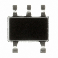
STLQ50C-R STMicroelectronics, STLQ50C-R Datasheet - Page 10

STLQ50C-R
Manufacturer Part Number
STLQ50C-R
Description
IC REG LDO 50MA ADJ SOT323-5
Manufacturer
STMicroelectronics
Datasheet
1.STLQ50C33R.pdf
(18 pages)
Specifications of STLQ50C-R
Regulator Topology
Positive Adjustable
Voltage - Output
1.22 ~ 11 V
Voltage - Input
2.3 ~ 12 V
Voltage - Dropout (typical)
0.4V @ 50mA
Number Of Regulators
1
Current - Output
50mA
Operating Temperature
-40°C ~ 125°C
Mounting Type
Surface Mount
Package / Case
SC-70-5, SC-88A, SOT-323-5, SOT-353, 5-TSSOP
Number Of Outputs
1
Polarity
Positive
Input Voltage Max
12 V
Output Voltage
1.222 V to 11 V
Output Type
Adjustable
Dropout Voltage (max)
0.7 V at 50 mA
Output Current
500 mA
Line Regulation
0.3 %
Load Regulation
0.15 %
Voltage Regulation Accuracy
2 %
Maximum Operating Temperature
+ 150 C
Mounting Style
SMD/SMT
Minimum Operating Temperature
- 40 C
Lead Free Status / RoHS Status
Lead free / RoHS Compliant
Current - Limit (min)
-
Lead Free Status / Rohs Status
Lead free / RoHS Compliant
Other names
497-5819-2
Available stocks
Company
Part Number
Manufacturer
Quantity
Price
Part Number:
STLQ50C-R
Manufacturer:
ST
Quantity:
20 000
7
7.1
7.2
10/18
Application information
The STLQ50 is a BiCMOS linear regulator specifically designed for operating in
environment with very low power consumption constraints. The very low quiescent current
of 3 µA is obtained with use of CMOS technology that makes the device suitable for those
application that have very long stand-by time. The very low power consumption allows
extending the battery life and the tiny packages (SOT323-5L or SOT23-5L) fulfil the space
saving requirements of battery powered equipments. Moreover the STLQ50 provides wide
input voltage operation from 2.5 V up to 12 V.
The P-MOS pass element allows also a very good drop-out figure: 0.7 V at full load and at
125 °C without affecting the consumption characteristics.
External components
The typical application schematic of STLQ50 is shown in
and output capacitors placed close to the device are needed in order to provide proper
operation. The device is stable with electrolytic and ceramic output capacitors having values
higher than 1 µF (see figure typical characteristics for stability details).
In the adjustable version (STLQ50) the output voltage is programmed using an external
resistor divider as shown in
and it can be calculated using the following formula:
V
where V
The sum between R
divider current at least. Lower value resistors will improve the noise performances but the
quiescent current will increase. Higher value resistors should be avoided because the ADJ
leakage current will influence the voltage set by the resistor divider making the above
formula no more valid.
The suggested design procedure is to choose R
following formula: R
Power dissipation
In order to ensure proper operation, the STLQ50 junction temperature should never exceed
125 °C, this limits the maximum power dissipation the regulator can sustain in any
application. The maximum power dissipation can be calculated as:
P
where T
T
R
data).
The power dissipation can be calculated simply as:
P
In every application condition, P
A
O
DMAX
D
thJA
is the ambient temperature;
= (V
= V
is the junction to ambient thermal resistance of the package
FB
= (T
I
JMAX
FB
- V
x (1+R
=1.222 V is the internal reference voltage;
JMAX
O
) x I
= 125 °C;
1
O
- T
/R
A
1
2
1
)/R
)
= (V
and R
thJA
O
/V
Figure
2
FB
resistors should be chosen in order to guarantee 1 µA of
-1) x R
D
must be lower than P
2. The output voltage can be adjusted from 1.22 to 11 V
2
2
= 1 MΩ and then calculate R
DMAX
Figure 1
.
-
(seeTable 4
Figure
2, a 1 µF input
1
thermal
using the


