STL52N25M5 STMicroelectronics, STL52N25M5 Datasheet
STL52N25M5
Specifications of STL52N25M5
Available stocks


Related parts for STL52N25M5


STL52N25M5 Summary of contents
Page 1
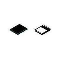
... Table 1. Device summary Order code STL52N25M5 September 2010 MDmesh™ V Power MOSFET R (1) DS(on max. < 0.065 Ω Figure 1. Marking 52N25M5 PowerFLAT™ (5x6) Doc ID 17819 Rev 1 STL52N25M5 PowerFLAT™ (5x6) Internal schematic diagram Package Packaging Tape and reel 1/12 www.st.com 12 ...
Page 2
... Contents Contents 1 Electrical ratings . . . . . . . . . . . . . . . . . . . . . . . . . . . . . . . . . . . . . . . . . . . . 3 2 Electrical characteristics . . . . . . . . . . . . . . . . . . . . . . . . . . . . . . . . . . . . . 4 2.1 Electrical characteristics (curves) 3 Test circuits 4 Package mechanical data . . . . . . . . . . . . . . . . . . . . . . . . . . . . . . . . . . . . . 9 5 Revision history . . . . . . . . . . . . . . . . . . . . . . . . . . . . . . . . . . . . . . . . . . . 11 2/ Doc ID 17819 Rev 1 STL52N25M5 . . . . . . . . . . . . . . . . . . . . . . . . . . . . 6 ...
Page 3
... STL52N25M5 1 Electrical ratings Table 2. Absolute maximum ratings Symbol V Gate- source voltage GS (1) I Drain current (continuous (1) I Drain current (continuous (1),(2) I Drain current (pulsed) DM (3) I Drain current (continuous (3) I Drain current (continuous (2),(3) I Drain current (pulsed) DM (1) P Total dissipation at T TOT (3) P Total dissipation at T ...
Page 4
... Figure 14) Doc ID 17819 Rev 1 Min. Typ 250 =125 ° 100 µ 0.055 Min. Typ. 1770 - 110 178 - 2 while V is rising from 0 oss DS while V is rising from 0 oss DS STL52N25M5 Max. Unit V 1 µA 100 µA 100 Ω 0.065 Max. Unit Ω ...
Page 5
... STL52N25M5 Table 6. Switching times Symbol t Voltage delay time d(V) t Voltage rise time r(V) t Current fall time f(i) t Crossing time c(off) Table 7. Source drain diode Symbol I Source-drain current SD (1) I Source-drain current (pulsed) SDM (2) V Forward on voltage SD t Reverse recovery time rr Q Reverse recovery charge ...
Page 6
... Electrical characteristics 2.1 Electrical characteristics (curves) Figure 2. Safe operating area Figure 4. Output characteristics Figure 6. Gate charge vs gate-source voltage Figure 7. 6/12 Figure 3. Thermal impedance Figure 5. Transfer characteristics Static drain-source on resistance Doc ID 17819 Rev 1 STL52N25M5 ...
Page 7
... STL52N25M5 Figure 8. Capacitance variations Figure 10. Normalized gate threshold voltage vs temperature Figure 12. Normalized B VDSS Figure 9. Figure 11. Normalized on resistance vs vs temperature Doc ID 17819 Rev 1 Electrical characteristics Output capacitance stored energy temperature 7/12 ...
Page 8
... AM01470v1 Figure 18. Switching time waveform V (BR)DSS Id 90%Vds Vgs 90%Vgs 10%Vds Vds AM01472v1 Doc ID 17819 Rev 1 STL52N25M5 12V 47kΩ 100nF I =CONST G 100Ω GMAX 2200 µF 2.7kΩ 47kΩ 1kΩ circuit 2200 3.3 µ D.U.T. Inductive Load Turn - off ...
Page 9
... STL52N25M5 4 Package mechanical data In order to meet environmental requirements, ST offers these devices in different grades of ® ECOPACK packages, depending on their level of environmental compliance. ECOPACK specifications, grade definitions and product status are available at: www.st.com. ECOPACK trademark. Doc ID 17819 Rev 1 Package mechanical data ® 9/12 ...
Page 10
... Doc ID 17819 Rev 1 STL52N25M5 inch MIN. TYP. MAX. 0.031 0.032 0.036 0.0007 0.0019 0.007 0.013 0.015 0.018 0.196 0.187 0.163 0.165 0.167 0.236 ...
Page 11
... STL52N25M5 5 Revision history Table 8. Document revision history Date 02-Aug-2010 Revision 1 First release. Doc ID 17819 Rev 1 Revision history Changes 11/12 ...
Page 12
... Australia - Belgium - Brazil - Canada - China - Czech Republic - Finland - France - Germany - Hong Kong - India - Israel - Italy - Japan - Malaysia - Malta - Morocco - Philippines - Singapore - Spain - Sweden - Switzerland - United Kingdom - United States of America 12/12 Please Read Carefully: © 2010 STMicroelectronics - All rights reserved STMicroelectronics group of companies www.st.com Doc ID 17819 Rev 1 STL52N25M5 ...