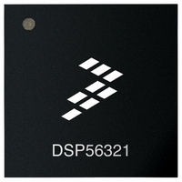
DSP56321VF220 Freescale Semiconductor, DSP56321VF220 Datasheet - Page 48

DSP56321VF220
Manufacturer Part Number
DSP56321VF220
Description
IC DSP 24BIT 220MHZ 196-BGA
Manufacturer
Freescale Semiconductor
Series
DSP563xxr
Type
Fixed Pointr
Datasheet
1.DSP56321VL200R2.pdf
(84 pages)
Specifications of DSP56321VF220
Interface
Host Interface, SSI, SCI
Clock Rate
220MHz
Non-volatile Memory
ROM (576 B)
On-chip Ram
576kB
Voltage - I/o
3.30V
Voltage - Core
1.60V
Operating Temperature
-40°C ~ 100°C
Mounting Type
*
Package / Case
196-MAPBGA
Device Core Size
24b
Format
Fixed Point
Clock Freq (max)
220MHz
Mips
220
Device Input Clock Speed
220MHz
Ram Size
576KB
Operating Supply Voltage (typ)
1.6/3.3V
Operating Supply Voltage (min)
1.5/3/3/3/3/3/3V
Operating Temp Range
-40C to 100C
Operating Temperature Classification
Industrial
Mounting
Surface Mount
Pin Count
196
Package Type
MA-BGA
Package
196MA-BGA
Numeric And Arithmetic Format
Fixed-Point
Maximum Speed
220 MHz
Device Million Instructions Per Second
220 MIPS
Lead Free Status / RoHS Status
Contains lead / RoHS non-compliant
Available stocks
Company
Part Number
Manufacturer
Quantity
Price
Company:
Part Number:
DSP56321VF220
Manufacturer:
XILINX
Quantity:
615
Company:
Part Number:
DSP56321VF220
Manufacturer:
Freescale Semiconductor
Quantity:
10 000
Specifications
2.4.11 JTAG Timing
2-28
Notes:
No.
500
501
502
503
504
505
506
507
508
509
510
511
512
513
1.
2.
TCK frequency of operation (1/(T
TCK cycle time in Crystal mode
TCK clock pulse width measured at 1.6 V
TCK rise and fall times
Boundary scan input data setup time
Boundary scan input data hold time
TCK low to output data valid
TCK low to output high impedance
TMS, TDI data setup time
TMS, TDI data hold time
TCK low to TDO data valid
TCK low to TDO high impedance
TRST assert time
TRST setup time to TCK low
V
All timings apply to OnCE module data transfers because it uses the JTAG port as an interface.
(Input)
CCQH
TCK
= 3.3 V ± 0.3 V, V
CCQL
503
Figure 2-28.
V
Characteristics
C
IH
= 1.6 V ± 0.1 V; T
× 3); absolute maximum 22 MHz)
DSP56321 Technical Data, Rev. 11
Table 2-14.
V
IL
Test Clock Input Timing Diagram
J
V
= –40°C to +100 °C, C
502
M
JTAG Timing
501
L
= 50 pF.
503
V
502
M
100.0
Min
45.0
20.0
24.0
25.0
40.0
0.0
0.0
5.0
0.0
0.0
5.0
0.0
0.0
All frequencies
Freescale Semiconductor
Max
22.0
40.0
40.0
44.0
44.0
3.0
—
—
—
—
—
—
—
—
Unit
MHz
ns
ns
ns
ns
ns
ns
ns
ns
ns
ns
ns
ns
ns


