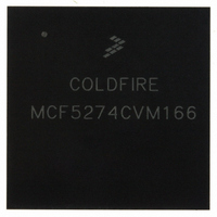
MCF5274CVM166 Freescale Semiconductor, MCF5274CVM166 Datasheet - Page 10

MCF5274CVM166
Manufacturer Part Number
MCF5274CVM166
Description
IC MPU 32BIT 166MHZ 256-MAPBGA
Manufacturer
Freescale Semiconductor
Series
MCF527xr
Datasheet
1.MCF5274LVM166J.pdf
(44 pages)
Specifications of MCF5274CVM166
Core Processor
Coldfire V2
Core Size
32-Bit
Speed
166MHz
Connectivity
EBI/EMI, Ethernet, I²C, SPI, UART/USART, USB
Peripherals
DMA, WDT
Number Of I /o
69
Program Memory Type
ROMless
Ram Size
64K x 8
Voltage - Supply (vcc/vdd)
1.4 V ~ 1.6 V
Oscillator Type
External
Operating Temperature
-40°C ~ 85°C
Package / Case
256-MAPBGA
Embedded Interface Type
I2C, SPI, USB, UART
Digital Ic Case Style
BGA
No. Of Pins
256
Operating Temperature Range
-40°C To +85°C
Processor Type
68K/ColdFire V2
Rohs Compliant
Yes
Family Name
MCF5xxx
Device Core
ColdFire
Device Core Size
32b
Frequency (max)
166MHz
Instruction Set Architecture
RISC
Operating Supply Voltage (max)
1.6V
Operating Supply Voltage (min)
1.4V
Operating Temp Range
-40C to 85C
Operating Temperature Classification
Industrial
Mounting
Surface Mount
Pin Count
256
Package Type
MA-BGA
Lead Free Status / RoHS Status
Lead free / RoHS Compliant
Eeprom Size
-
Program Memory Size
-
Data Converters
-
Lead Free Status / Rohs Status
Compliant
Available stocks
Company
Part Number
Manufacturer
Quantity
Price
Company:
Part Number:
MCF5274CVM166
Manufacturer:
Freescale Semiconductor
Quantity:
10 000
Design Recommendations
5.2.1
Figure 2
(PLLV
The relationship between SDV
SDV
5.2.1.1
If OV
output drivers connected to the OV
long after OV
SDV
protection diodes. The rise times on the power supplies should be slower than 1 μs to avoid turning on the
internal ESD protection clamp diodes.
The recommended power up sequence is as follows:
10
1. Use 1 μs or slower rise time for all supplies.
2. V
DD
DD,
DD
DD
ramps with OV
use a low drop-out voltage regulator.
(2.5V or 3.3V) and OV
/SDV
or PLLV
shows situations in sequencing the I/O V
DD
), and Core V
Supply Voltage Sequencing and Separation Cautions
/PLLV
Power Up Sequence
DD
DD
/SDV
DD
are powered up with V
3.3V
2.5V
1.5V
DD
MCF5275 Integrated Microprocessor Family Hardware Specification, Rev. 4
by more than 0.4 V during power ramp-up or high current will be in the internal ESD
Notes:
0
Figure 2. Supply Voltage Sequencing and Separation Cautions
DD
and OV
DD
DD
1.
2.
3.
4.
/SD V
VDD should not exceed OVDD, SDVDD or PLLVDD by more than
0.4 V at any time, including power-up.
Recommended that VDD should track OVDD/SDVDD/PLLVDD up to
0.9 V, then separate for completion of ramps.
Input voltage must not be greater than the supply voltage (OVDD, SDVDD,
VDD, or PLLVDD) by more than 0.5 V at any time, including during power-up.
Use 1 ms or slower rise time for all supplies.
powers up before V
(V
DD
DD
1
DD
DD
DD
).
/SDV
and OV
2
DD
going to the higher external voltages. One way to accomplish this is to
are specified relative to V
/SDV
DD
DD
DD
should track up to 0.9 V, then separate for the completion of
DD
Supplies Stable
at 0 V, then the sense circuits in the I/O pads cause all pad
is non-critical during power-up and power-down sequences.
DD
to be in a high impedance state. There is no limit on how
must powered up. V
DD
(OV
DD
), SDRAM V
DD
.
DD
OV
V
SDV
should not lead the OV
DD
DD
DD
,
DD
, SDV
(SDV
(2.5V)
DD
Time
DD
Freescale Semiconductor
, PLLV
), PLL V
DD
DD
DD
,


