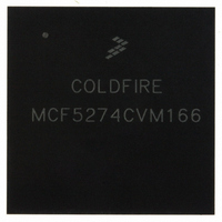
MCF5274CVM166 Freescale Semiconductor, MCF5274CVM166 Datasheet - Page 30

MCF5274CVM166
Manufacturer Part Number
MCF5274CVM166
Description
IC MPU 32BIT 166MHZ 256-MAPBGA
Manufacturer
Freescale Semiconductor
Series
MCF527xr
Datasheet
1.MCF5274LVM166J.pdf
(44 pages)
Specifications of MCF5274CVM166
Core Processor
Coldfire V2
Core Size
32-Bit
Speed
166MHz
Connectivity
EBI/EMI, Ethernet, I²C, SPI, UART/USART, USB
Peripherals
DMA, WDT
Number Of I /o
69
Program Memory Type
ROMless
Ram Size
64K x 8
Voltage - Supply (vcc/vdd)
1.4 V ~ 1.6 V
Oscillator Type
External
Operating Temperature
-40°C ~ 85°C
Package / Case
256-MAPBGA
Embedded Interface Type
I2C, SPI, USB, UART
Digital Ic Case Style
BGA
No. Of Pins
256
Operating Temperature Range
-40°C To +85°C
Processor Type
68K/ColdFire V2
Rohs Compliant
Yes
Family Name
MCF5xxx
Device Core
ColdFire
Device Core Size
32b
Frequency (max)
166MHz
Instruction Set Architecture
RISC
Operating Supply Voltage (max)
1.6V
Operating Supply Voltage (min)
1.4V
Operating Temp Range
-40C to 85C
Operating Temperature Classification
Industrial
Mounting
Surface Mount
Pin Count
256
Package Type
MA-BGA
Lead Free Status / RoHS Status
Lead free / RoHS Compliant
Eeprom Size
-
Program Memory Size
-
Data Converters
-
Lead Free Status / Rohs Status
Compliant
Available stocks
Company
Part Number
Manufacturer
Quantity
Price
Company:
Part Number:
MCF5274CVM166
Manufacturer:
Freescale Semiconductor
Quantity:
10 000
Electrical Characteristics
Figure 13
30
1
2
3
4
5
6
7
DD13 DQS input read preamble width (t
DD14 DQS input read postamble width (t
DD15 DQS output write preamble width (t
DD16 DQS output write postamble width (t
NUM
All timing specifications are based on taking into account, a 25pF load on the SDRAM output pins.
DDR_CLKOUT operates at half the frequency of the PLLMRFM output and the ColdFire core.
t
D[31:24] is relative to SD_DQS3 and D[23:16] is relative to SD_DQS2.
The first data beat is valid before the first rising edge of SD_DQS and after the SD_DQS write preamble. The remaining
data beats are valid for each subsequent SD_DQS edge
Data input skew is derived from each SD_DQS clock edge. It begins with a SD_DQS transition and ends when the last data
line becomes valid. This input skew must include DDR memory output skew and system level board skew (due to routing or
other factors).
Data input hold is derived from each SD_DQS clock edge. It begins with a SD_DQS transition and ends when the first data
line becomes invalid.
CKH
+ t
CKL
DDR_CLKOUT
DDR_CLKOUT
shows a DDR SDRAM write cycle.
must be less than or equal to t
MCF5275 Integrated Microprocessor Family Hardware Specification, Rev. 4
Figure 12. DDR_CLKOUT and DDR_CLKOUT Crossover Timing
Characteristic
Table 15. DDR Timing (continued)
RPRE
RPST
CK
WPRE
WPST
1
.
)
)
)
)
Symbol
t
t
t
t
WPRE
WPST
RPRE
RPST
0.25
Min
0.9
0.4
0.4
Freescale Semiconductor
V
V
V
IX
MP
IX
Max
1.1
0.6
0.6
—
V
ID
Unit
t
t
t
t
CK
CK
CK
CK


