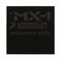
MC9328MXLVP20 Freescale Semiconductor, MC9328MXLVP20 Datasheet - Page 7

MC9328MXLVP20
Manufacturer Part Number
MC9328MXLVP20
Description
IC MCU I.MX 200MHZ 225-MAPBGA
Manufacturer
Freescale Semiconductor
Series
i.MXLr
Datasheet
1.MC9328MXLVP15R2.pdf
(90 pages)
Specifications of MC9328MXLVP20
Core Processor
ARM9
Core Size
32-Bit
Speed
200MHz
Connectivity
EBI/EMI, I²C, Memory Stick, MMC/SD, SPI, SSI, UART/USART, USB
Peripherals
DMA, I²S, LCD, POR, PWM, WDT
Number Of I /o
97
Program Memory Type
ROMless
Voltage - Supply (vcc/vdd)
1.7 V ~ 3.3 V
Oscillator Type
External
Operating Temperature
0°C ~ 70°C
Package / Case
225-MAPBGA
Lead Free Status / RoHS Status
Lead free / RoHS Compliant
Eeprom Size
-
Ram Size
-
Program Memory Size
-
Data Converters
-
Available stocks
Company
Part Number
Manufacturer
Quantity
Price
Company:
Part Number:
MC9328MXLVP20
Manufacturer:
Freescale Semiconductor
Quantity:
10 000
Company:
Part Number:
MC9328MXLVP20R2
Manufacturer:
Freescale Semiconductor
Quantity:
10 000
Freescale Semiconductor
CLS
REV
SPI1_MOSI
SPI1_MISO
SPI1_SS
SPI1_SCLK
SPI1_SPI_RDY
SPI2_TXD
SPI2_RXD
SPI2_SS
SPI2_SCLK
TIN
TMR2OUT
USBD_VMO
USBD_VPO
USBD_VM
USBD_VP
USBD_SUSPND
USBD_RCV
USBD_ROE
USBD_AFE
SD_CMD
SD_CLK
Signal Name
Start signal output for gate driver. This signal is an inverted version of PS (Sharp panel dedicated
signal).
Signal for common electrode driving signal preparation (Sharp panel dedicated signal).
Master Out/Slave In
Slave In/Master Out
Slave Select (Selectable polarity)
Serial Clock
Serial Data Ready
SPI2 Master TxData Output—This signal is multiplexed with a GPI/O pin yet shows up as a primary or
alternative signal in the signal multiplex scheme table. Please refer to the SPI and GPIO chapters in
the MC9328MXL Reference Manual for information about how to bring this signal to the assigned pin.
SPI2 Master RxData Input—This signal is multiplexed with a GPI/O pin yet shows up as a primary or
alternative signal in the signal multiplex scheme table. Please refer to the SPI and GPIO chapters in
the MC9328MXL Reference Manual for information about how to bring this signal to the assigned pin.
SPI2 Slave Select—This signal is multiplexed with a GPI/O pin yet shows up as a primary or alternative
signal in the signal multiplex scheme table. Please refer to the SPI and GPIO chapters in the
MC9328MXL Reference Manual for information about how to bring this signal to the assigned pin.
SPI2 Serial Clock—This signal is multiplexed with a GPI/O pin yet shows up as a primary or alternative
signal in the signal multiplex scheme table. Please refer to the SPI and GPIO chapters in the
MC9328MXL Reference Manual for information about how to bring this signal to the assigned pin.
Timer Input Capture or Timer Input Clock—The signal on this input is applied to both timers
simultaneously.
Timer 2 Output
USB Minus Output
USB Plus Output
USB Minus Input
USB Plus Input
USB Suspend Output
USB Receive Data
USB OE
USB Analog Front End Enable
SD Command—If the system designer does not wish to make use of the internal pull-up, via the Pull-up
enable register, a 4.7K–69K external pull up resistor must be added.
MMC Output Clock
Table 2. i.MXL Signal Descriptions (Continued)
MC9328MXL Technical Data, Rev. 8
General Purpose Timers
Secure Digital Interface
SPI 1 and SPI 2
USB Device
Function/Notes
Signals and Connections
7


