1321XDSK-BDM Freescale Semiconductor, 1321XDSK-BDM Datasheet - Page 55
1321XDSK-BDM
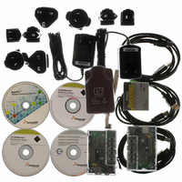
Manufacturer Part Number
1321XDSK-BDM
Description
KIT STARTER DEV 1321X W/USB
Manufacturer
Freescale Semiconductor
Type
Sensor Demor
Specifications of 1321XDSK-BDM
Frequency
2.4GHz
Wireless Frequency
2.4 GHz
Interface Type
SPI
Modulation
DSSS OQPSK
Security
128 bit AES
Operating Voltage
2 VDC to 3.4 VDC
Output Power
2 dBm
Antenna
F-Antenna
Operating Temperature Range
- 40 C to + 85 C
For Use With/related Products
MC1321x
Lead Free Status / RoHS Status
Contains lead / RoHS compliant by exemption


1
2
3
4
5
6
7
8
9
10
Freescale Semiconductor
Num
All ACCURACY numbers are based on processor and system being in WAIT state (very little activity and no IO switching) and
that adequate low-pass filtering is present on analog input pins (filter with 0.01 μF to 0.1 μF capacitor between analog input
and V
will vary based on board layout and the type and magnitude of the activity.
This is the conversion time for subsequent conversions in continuous convert mode. Actual conversion time for single
conversions or the first conversion in continuous mode is extended by one ATD clock cycle and 2 bus cycles due to starting
the conversion and setting the CCF flag. The total conversion time in Bus Cycles for a conversion is:
fully charge the input circuitry of the ATD resulting in accuracy error.
Analog input must be between V
full scale error (E
The resolution is the ideal step size or 1LSB = (V
Differential non-linearity is the difference between the current code width and the ideal code width (1LSB). The current code
width is the difference in the transition voltages to and from the current code.
Integral non-linearity is the difference between the transition voltage to the current code and the adjusted ideal transition
voltage for the current code. The adjusted ideal transition voltage is (Current Code–1/2)*(1/((V
Zero-scale error is the difference between the transition to the first valid code and the ideal transition to that code. The Ideal
transition voltage to a given code is (Code–1/2)*(1/(V
Full-scale error is the difference between the transition to the last valid code and the ideal transition to that code. The ideal
transition voltage to a given code is (Code–1/2)*(1/(V
Input leakage error is error due to input leakage across the real portion of the impedance of the network driving the analog pin.
Reducing the impedance of the network reduces this error.
10
11
12
R
1
2
3
4
5
6
7
8
9
AS
is the real portion of the impedance of the network driving the analog input pin. Values greater than this amount may not
REFL
ATD conversion clock
frequency
Conversion cycles
(continuous convert)
Conversion time
Source impedance at
input
Analog Input Voltage
Ideal resolution (1 LSB)
Differential non-linearity
Integral non-linearity
Zero-scale error
Full-scale error
Input leakage error
Total unadjusted
error
). Failure to observe these guidelines may result in system or microcontroller noise causing accuracy errors which
11
3
Characteristic
SC Bus Cycles = ((PRS+1)*2) * (28+1) + 2
FS
).
9
8
10
2
7
4
5
6
Table 15. ATD Timing/Performance Characteristics
REFL
Symbol
f
ATDCLK
and V
T
CCP
RES
V
DNL
R
E
E
E
INL
E
MC13211/212/213 Technical Data, Rev. 1.8
conv
AIN
AS
ZS
FS
TU
IL
REFH
1.80V < V
1.80V < V
1.80V < V
1.80 V < V
2.08V < V
2.08V < V
2.08V < V
1.80V < V
1.80V < V
1.80V < V
1.80V < V
1.80V < V
for valid conversion. Values greater than V
REFH
REFH
REFH
–V
Condition
REFL
DDAD
DDAD
DDAD
–V
–V
DDAD
DDAD
DDAD
DDAD
DDAD
DDAD
DDAD
DDAD
DDAD
REFL
REFL
)/1024
< 2.08V
< 2.08V
< 2.08V
< 3.6V
< 3.6V
< 3.6V
< 3.6V
< 3.6V
< 3.6V
< 3.6V
< 3.6V
CC Bus Cycles = ((PRS+1)*2) * (28)
< 3.6V
)).
)).
V
2.031
1.758
14.0
28.0
Min
0.5
0.5
REFL
28
—
—
—
—
—
—
—
+0.05
+0.5
+0.5
+0.4
+0.4
+1.1
Typ
28
1
—
—
—
—
—
—
—
REFH
REFH
will convert to $3FF less the
+E
V
3.516
2.031
FS
Max
60.0
60.0
+1.0
+1.0
+1.0
+1.0
+2.5
<30
REFH
2.0
1.0
10
+5
)–(V
REFL
+E
ATDCLK
cycles
MHz
Unit
LSB
LSB
LSB
LSB
LSB
LSB
ZS
mV
μS
kΩ
V
))).
55
Related parts for 1321XDSK-BDM
Image
Part Number
Description
Manufacturer
Datasheet
Request
R

Part Number:
Description:
KIT STARTER DEVELOPER 1321X
Manufacturer:
Freescale Semiconductor
Datasheet:

Part Number:
Description:
Manufacturer:
Freescale Semiconductor, Inc
Datasheet:
Part Number:
Description:
Manufacturer:
Freescale Semiconductor, Inc
Datasheet:
Part Number:
Description:
Manufacturer:
Freescale Semiconductor, Inc
Datasheet:
Part Number:
Description:
Manufacturer:
Freescale Semiconductor, Inc
Datasheet:
Part Number:
Description:
Manufacturer:
Freescale Semiconductor, Inc
Datasheet:
Part Number:
Description:
Manufacturer:
Freescale Semiconductor, Inc
Datasheet:
Part Number:
Description:
Manufacturer:
Freescale Semiconductor, Inc
Datasheet:
Part Number:
Description:
Manufacturer:
Freescale Semiconductor, Inc
Datasheet:
Part Number:
Description:
Manufacturer:
Freescale Semiconductor, Inc
Datasheet:
Part Number:
Description:
Manufacturer:
Freescale Semiconductor, Inc
Datasheet:
Part Number:
Description:
Manufacturer:
Freescale Semiconductor, Inc
Datasheet:
Part Number:
Description:
Manufacturer:
Freescale Semiconductor, Inc
Datasheet:
Part Number:
Description:
Manufacturer:
Freescale Semiconductor, Inc
Datasheet:
Part Number:
Description:
Manufacturer:
Freescale Semiconductor, Inc
Datasheet: