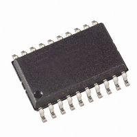
ATA5760N3-TGQY Atmel, ATA5760N3-TGQY Datasheet - Page 14

ATA5760N3-TGQY
Manufacturer Part Number
ATA5760N3-TGQY
Description
IC RCVR ASK/FSK 868MHZ 20SOIC
Manufacturer
Atmel
Datasheet
1.ATA5760N-TGSY.pdf
(41 pages)
Specifications of ATA5760N3-TGQY
Frequency
868MHz
Sensitivity
-110dBm
Data Rate - Maximum
10 kBaud
Modulation Or Protocol
ASK, FSK
Applications
Telemetering and Security Systems
Current - Receiving
7.8mA
Data Interface
PCB, Surface Mount
Antenna Connector
PCB, Surface Mount
Voltage - Supply
4.5 V ~ 5.5 V
Operating Temperature
-40°C ~ 105°C
Package / Case
20-SOIC (0.300", 7.50mm Width)
Operating Temperature (min)
-40C
Operating Temperature (max)
105C
Operating Temperature Classification
Industrial
Operating Supply Voltage (min)
4.5V
Operating Supply Voltage (typ)
5V
Operating Supply Voltage (max)
5.5V
Lead Free Status / RoHS Status
Lead free / RoHS Compliant
Features
-
Memory Size
-
Lead Free Status / Rohs Status
Compliant
Figure 8-6.
8.4
8.5
8.6
14
Duration of the Bit Check
Receiving Mode
Digital Signal Processing
Bit check
(Lim_min = 14, Lim_max = 24)
IC_ACTIVE
Dem_out
Bit-check-
counter
ATA5760/ATA5761
Timing Diagram for Failed Bit Check (Condition: CV_Lim
Start-up mode
T
If no transmitter signal is present during the bit check, the output of the ASK/FSK demodulator
delivers random signals. The bit check is a statistical process and T
Therefore, an average value for T
depends on the selected baud-rate range and on T
value for T
In the presence of a valid transmitter signal, T
nal, f
a longer period for T
If the bit check was successful for all bits specified by N
mode. According to
that case and the data clock is available after the start bit has been detected (see
page
the data clock at pin DATA_CLK. The receiver stays in that condition until it is switched back to
polling mode explicitly.
The data from the ASK/FSK demodulator (Dem_out) is digitally processed in different ways and
as a result converted into the output signal data. This processing depends on the selected
baud-rate range (BR_Range).
extended clock cycle T
state only after T
is always an integral multiple of T
The minimum time period between two edges of the data signal is limited to t
implies an efficient suppression of spikes at the DATA output. At the same time it limits the max-
imum frequency of edges at DATA. This eases the interrupt handling of a connected
microcontroller.
The maximum time period for DATA to stay Low is limited to T
employed to ensure a finite response time in programming or switching off the receiver via pin
DATA. T
data stream.
receiver has switched to receiving mode.
0
Start-up
Sig
19). A connected microcontroller can be woken up by the negative edge at pin DATA or by
, and the count of the checked bits, N
DATA_L_max
1
Bit-check
2 3 4 5 6
Figure 8-9 on page 15
XClk
resulting in a lower current consumption in polling mode.
is thereby longer than the maximum time period indicated by the transmitter
7
Bit-check
Figure 8-2 on page
has elapsed. The edge-to-edge time period t
1
XClk
2
3
. This clock is also used for the bit-check counter. Data can change its
4 5
Bit-check mode
requiring a higher value for the transmitter pre-burst T
T
6 7 8 9
Bit-check
Figure 8-7
XClk
Bit-check
10
.
gives an example where Dem_out remains Low after the
1/2 Bit
11 12
11, the internal data signal is switched to pin DATA in
13 14 15 16 17 18 19
is given in the electrical characteristics. T
Bit-check
illustrates how Dem_out is synchronized by the
Bit-check
Lim_max)
. A higher value for N
Clk
. A higher baud-rate range causes a lower
is dependent on the frequency of that sig-
20
Bit check failed ( CV_Lim
Bit-check
21 22 23 24
, the receiver switches to receiving
ee
Bit-check
of the Data signal as a result
DATA_L_max
Sleep mode
Bit-check
T
0
varies for each check.
Sleep
Lim_max )
ee
. This function is
thereby results in
Preburst
T
4896D–RKE–08/08
Figure 9-1 on
DATA_min
.
Bit-check
. This


