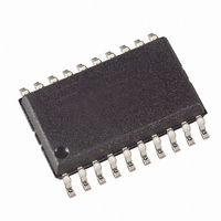
ATA5760N3-TGQY Atmel, ATA5760N3-TGQY Datasheet - Page 34

ATA5760N3-TGQY
Manufacturer Part Number
ATA5760N3-TGQY
Description
IC RCVR ASK/FSK 868MHZ 20SOIC
Manufacturer
Atmel
Datasheet
1.ATA5760N-TGSY.pdf
(41 pages)
Specifications of ATA5760N3-TGQY
Frequency
868MHz
Sensitivity
-110dBm
Data Rate - Maximum
10 kBaud
Modulation Or Protocol
ASK, FSK
Applications
Telemetering and Security Systems
Current - Receiving
7.8mA
Data Interface
PCB, Surface Mount
Antenna Connector
PCB, Surface Mount
Voltage - Supply
4.5 V ~ 5.5 V
Operating Temperature
-40°C ~ 105°C
Package / Case
20-SOIC (0.300", 7.50mm Width)
Operating Temperature (min)
-40C
Operating Temperature (max)
105C
Operating Temperature Classification
Industrial
Operating Supply Voltage (min)
4.5V
Operating Supply Voltage (typ)
5V
Operating Supply Voltage (max)
5.5V
Lead Free Status / RoHS Status
Lead free / RoHS Compliant
Features
-
Memory Size
-
Lead Free Status / Rohs Status
Compliant
17. Electrical Characteristics (Continued)
All parameters refer to GND, T
(For typical values: V
18. Electrical Characteristics (continued)
All parameters refer to GND, T
(For typical values: V
Parameter
Data Clock (see
Minimum
delay time
between
edge at DATA
and
DATA_CLK
Pulse width
of negative
pulse at pin
DATA_CLK
34
Parameters
Current consumption
LNA, Mixer, Polyphase Lowpass and IF Amplifier (Input Matched According to
Third-order intercept point
LO spurious emission
System noise figure
LNA_IN input impedance
1 dB compression point
Image rejection
Maximum input level
ATA5760/ATA5761
Test Conditions
BR_Range =
BR_Range0
BR_Range1
BR_Range2
BR_Range3
BR_Range =
BR_Range0
BR_Range1
BR_Range2
BR_Range3
Figure 10-2 on page 22
S
S
= 5V, T
= 5V, T
amb
amb
t
amb
amb
P_DATA_CLK
Symbol
t
Delay2
= 25°C)
= 25°C)
= –40°C to +105°C, V
= –40°C to +105°C, V
Test Conditions
Sleep mode
(XTO and polling logic active)
IC active (start-up-, bit-check-,
receiving mode) Pin DATA = H
FSK
ASK
LNA/mixer/IF amplifier
Required according to I-ETS 300220
With power matching |S11| < –10 dB
At 868.3 MHz
At 915 MHz
Within the complete image band
BER
FSK mode
ASK mode
and
Figure 10-3 on page
Min.
66.1
33.0
16.5
8.3
0
0
0
0
10
f
RF
-3
,
= 868.3 MHz
Typ.
S
S
= 4.5V to 5.5V, f
= 4.5V to 5.5V, f
Max.
16.5
66.1
33.0
16.5
8.3
4.1
2.1
8.3
22)
Min.
15.7
7.8
63
31
0
0
0
0
0
0
f
= 868.3 MHz and f
= 868.3 MHz and f
RF
= 915 MHz
Symbol
Typ.
Zi
P
IS
IP
IS
IS
IIP3
LNA_IN
in_max
NF
LORF
1db
off
on
Figure 14-1 on page 30
Max.
16.7
1.96
15.7
7.8
3.9
7.8
63
31
0
0
Min.
20
= 915 MHz, unless otherwise specified.
= 915 MHz, unless otherwise specified.
4
4
4
4
Min.
0
0
0
0
T
T
T
T
XClk
XClk
XClk
XClk
Variable Oscillator
200 || 3.2
200 || 3.2
Typ.
170
–16
–70
–25
7.8
7.4
30
5
Typ.
Referred to RFIN)
Max.
276
–57
–10
–10
9.9
9.6
1
1
1
1
4
4
4
4
4896D–RKE–08/08
Max.
T
T
T
T
T
T
T
T
XClk
XClk
XClk
XClk
XClk
XClk
XClk
XClk
dBm
dBm
dBm
dBm
dBm
Unit
mA
mA
µA
dB
dB
|| pF
|| pF
Unit
µs
µs
µs
µs
µs
µs
µs
µs


