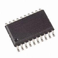
ATA5760N3-TGQY Atmel, ATA5760N3-TGQY Datasheet - Page 20

ATA5760N3-TGQY
Manufacturer Part Number
ATA5760N3-TGQY
Description
IC RCVR ASK/FSK 868MHZ 20SOIC
Manufacturer
Atmel
Datasheet
1.ATA5760N-TGSY.pdf
(41 pages)
Specifications of ATA5760N3-TGQY
Frequency
868MHz
Sensitivity
-110dBm
Data Rate - Maximum
10 kBaud
Modulation Or Protocol
ASK, FSK
Applications
Telemetering and Security Systems
Current - Receiving
7.8mA
Data Interface
PCB, Surface Mount
Antenna Connector
PCB, Surface Mount
Voltage - Supply
4.5 V ~ 5.5 V
Operating Temperature
-40°C ~ 105°C
Package / Case
20-SOIC (0.300", 7.50mm Width)
Operating Temperature (min)
-40C
Operating Temperature (max)
105C
Operating Temperature Classification
Industrial
Operating Supply Voltage (min)
4.5V
Operating Supply Voltage (typ)
5V
Operating Supply Voltage (max)
5.5V
Lead Free Status / RoHS Status
Lead free / RoHS Compliant
Features
-
Memory Size
-
Lead Free Status / Rohs Status
Compliant
20
ATA5760/ATA5761
Figure 9-4.
The delay of the data clock is calculated as follows: t
t
depends on the capacitive load C
falling edge, t
on page 21
Data_Out, the data clock is issued after an additional delay t
Note that the capacitive load at pin DATA is limited. If the maximum tolerated capacitive load at
pin DATA is exceeded, the data clock disappears (see section
Figure 9-5.
DATA_CLK
Dem_out
Data_out (DATA)
Delay1
is the delay between the internal signals Data_Out and Data_In. For the rising edge, t
and
Delay1
Output of the Data Clock After a Successful Bit Check
Timing Characteristic of the Data Clock (Rising Edge on Pin DATA)
Serial bi-directional
data line
Data_In
DATA_CLK
Data_Out
Figure 13-2 on page
depends additionally on the external voltage V
'1'
Receiving mode,
bit check active
Bit check ok
'1'
V
V
IH
II
= 0.35
= 0.65
L
'1'
at pin DATA and the external pull-up resistor R
V
V
V
S
X
S
28). When the level of Data_In is equal to the level of
'1'
t
Delay1
t
Delay
'1'
t
Delay2
t
Data
P_Data_Clk
Delay
Start bit
'0'
= t
Receiving mode,
data clock control
logic active
Delay1
Delay2
'1'
“Data Interface” on page
.
+ t
X
'1'
Delay2
(see
Figure
'0'
'1'
9-5,
4896D–RKE–08/08
pup
Figure 9-6
'0'
. For the
29).
Delay1


