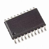
ATA5760N3-TGQY Atmel, ATA5760N3-TGQY Datasheet - Page 28

ATA5760N3-TGQY
Manufacturer Part Number
ATA5760N3-TGQY
Description
IC RCVR ASK/FSK 868MHZ 20SOIC
Manufacturer
Atmel
Datasheet
1.ATA5760N-TGSY.pdf
(41 pages)
Specifications of ATA5760N3-TGQY
Frequency
868MHz
Sensitivity
-110dBm
Data Rate - Maximum
10 kBaud
Modulation Or Protocol
ASK, FSK
Applications
Telemetering and Security Systems
Current - Receiving
7.8mA
Data Interface
PCB, Surface Mount
Antenna Connector
PCB, Surface Mount
Voltage - Supply
4.5 V ~ 5.5 V
Operating Temperature
-40°C ~ 105°C
Package / Case
20-SOIC (0.300", 7.50mm Width)
Operating Temperature (min)
-40C
Operating Temperature (max)
105C
Operating Temperature Classification
Industrial
Operating Supply Voltage (min)
4.5V
Operating Supply Voltage (typ)
5V
Operating Supply Voltage (max)
5.5V
Lead Free Status / RoHS Status
Lead free / RoHS Compliant
Features
-
Memory Size
-
Lead Free Status / Rohs Status
Compliant
13. Programming the Configuration Register
Figure 13-1. Timing of the Register Programming
28
Serial bi-directional
data line
ATA5760/ATA5761
Out1
(microcontroller)
Data_out (DATA)
IC_ACTIVE
X
X
Figure 13-2. Data Interface
The configuration registers are programmed serially via the bi-directional data line according to
Figure 13-1
To start programming, the serial data line DATA is pulled to Low for the time period t1 by the
microcontroller. When DATA has been released, the receiver becomes the master device. When
the programming delay period t2 has elapsed, it emits 15 subsequent synchronization pulses
with the pulse length t3. After each of these pulses, a programming window occurs. The delay
until the program window starts is determined by t4, the duration is defined by t5. Within the pro-
gramming window, the individual bits are set. If the microcontroller pulls down pin DATA for the
time period t7 during t5, the according bit is set to ’0’. If no programming pulse t7 is issued, this
bit is set to ’1’. All 15 bits are subsequently programmed this way. The time frame to program a
bit is defined by t6.
Receiving
mode
Data_In
Data_out
V
S
= 4.5 V to 5.5 V
t1
0 V/5 V
and
t2
Figure
Interface
t3
Input -
(Start bit)
t4
Bit 1
("0")
13-2.
t5
t7
t6
ATA5760/
ATA5761
0 ... 20 V
Programming frame
(Register-
Bit 2
("1")
select)
I
D
DATA
Serial bi-directional data line
V
R
C
pup
X
L
= 5 V to 20 V
(Poll8)
Bit 14
("0")
(Stop bit)
I/O
Bit 15
("0")
Microcontroller
t8
t9
Sleep
mode
T
Out1 (microcontroller )
Sleep
Start-up
4896D–RKE–08/08
T
mode
Start-up


