UAA3220TS/V1,118 NXP Semiconductors, UAA3220TS/V1,118 Datasheet - Page 16
UAA3220TS/V1,118
Manufacturer Part Number
UAA3220TS/V1,118
Description
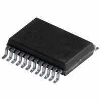
IC RECEIVER ASK/FSK 24SSOP
Manufacturer
NXP Semiconductors
Type
Receiverr
Datasheet
1.UAA3220TSV1118.pdf
(32 pages)
Specifications of UAA3220TS/V1,118
Package / Case
24-SSOP
Frequency
250MHz ~ 920MHz
Sensitivity
-119dBm
Modulation Or Protocol
ASK, FSK
Applications
Car Alarm Systems, RKE
Current - Receiving
4.3mA
Data Interface
PCB, Surface Mount
Antenna Connector
PCB, Surface Mount
Voltage - Supply
2.7 V ~ 5.5 V
Operating Temperature
-40°C ~ 85°C
Operating Frequency
290 MHz
Operating Supply Voltage
3.3 V or 5 V
Maximum Operating Temperature
+ 85 C
Minimum Operating Temperature
- 40 C
Mounting Style
SMD/SMT
Lead Free Status / RoHS Status
Lead free / RoHS Compliant
Features
-
Memory Size
-
Data Rate - Maximum
-
Lead Free Status / Rohs Status
Lead free / RoHS Compliant
Other names
935261031118
UAA3220TSDB-T
UAA3220TSDB-T
UAA3220TSDB-T
UAA3220TSDB-T


Philips Semiconductors
Table 3 Tests and results
P
power from signal generator 2 at the input of the test board.
Notes
1. The voltage at pin PWD of the test circuit alternates between operating mode: on (50 ms; 0 V) and off (138 ms; V
2. Probe of spectrum analyzer connected to pin FA (pin 22).
3. Spectrum analyzer connected to the input of the test board.
1999 Jan 22
handbook, full pagewidth
ASK sensitivity into
pin MIXIN (see Fig.5)
FSK sensitivity into
pin MIXIN (see Fig.5)
Maximum input power
for ASK (see Fig.5)
Maximum input power
for FSK (see Fig.5)
Receiver turn-on
time; see note 1 and
Fig.4
Interception point
(mixer + PMA)
see note 2 and Fig.6
Spurious radiation;
see note 3 and Fig.7
1
Frequency Shift Keying (FSK)/Amplitude
Shift Keying (ASK) receiver
is the maximum available power from signal generator 1 at the input of the test board; P
see Fig.4.
TEST
V PWD
(V)
2.7
0
0
modulated test signal 1;
P
f
P
f
modulated test signal 2;
P
modulated test signal 1;
P
modulated test signal 2;
P
modulated test
signal 1 or 2;
P
test signal 3;
P
i(RF)
i(RF)
1
1
1
1
1
1
1
= P
= 40 dBm
= 433.92 MHz;
= 868.35 MHz
113 dBm for
110 dBm for
100 dBm
22 dBm
6 dBm
ref
50
Fig.4 Timing diagram for pulsed power down voltage.
+ 3 dB
1
GENERATOR
188
test signal 4;
P
2
= P
16
238
2
1
BER
(e.g. 60 bit errors per second for 2000 bits/s)
BER
(e.g. 60 bit errors per second for 2000 bits/s)
BER
(e.g. 60 bit errors per second for 2000 bits/s)
BER
(e.g. 60 bit errors per second for 2000 bits/s)
check that the first 10 bits are correct;
error counting is started 10 ms after power down
is switched into operating mode on
measure with high impedance probe at pin FA
no spurious signals (25 MHz to 1 GHz) with level
higher than maximum P
IP3
PMA
3
3
3
3
376
=
10
10
10
10
P
1
2
2
2
2
+
IM3
--------- - dBm
2
426
RESULT
2
is the maximum available
t (ms)
SPUR
MGM745
(for IM3 see Fig.6)
UAA3220TS
Product specification
CC
);
Related parts for UAA3220TS/V1,118
Image
Part Number
Description
Manufacturer
Datasheet
Request
R

Part Number:
Description:
Manufacturer:
NXP Semiconductors
Datasheet:

Part Number:
Description:
IC RECEIVER ASK/FSK 24SSOP
Manufacturer:
NXP Semiconductors
Datasheet:
Part Number:
Description:
Frequency Shift Keying Fsk/amplitude Shift Keying Ask Receiver
Manufacturer:
NXP Semiconductors
Datasheet:

Part Number:
Description:
Frequency Shift Keying FSK/Amplitude Shift Keying ASK receiver
Manufacturer:
PHILIPS [NXP Semiconductors]
Datasheet:
Part Number:
Description:
NXP Semiconductors designed the LPC2420/2460 microcontroller around a 16-bit/32-bitARM7TDMI-S CPU core with real-time debug interfaces that include both JTAG andembedded trace
Manufacturer:
NXP Semiconductors
Datasheet:

Part Number:
Description:
NXP Semiconductors designed the LPC2458 microcontroller around a 16-bit/32-bitARM7TDMI-S CPU core with real-time debug interfaces that include both JTAG andembedded trace
Manufacturer:
NXP Semiconductors
Datasheet:
Part Number:
Description:
NXP Semiconductors designed the LPC2468 microcontroller around a 16-bit/32-bitARM7TDMI-S CPU core with real-time debug interfaces that include both JTAG andembedded trace
Manufacturer:
NXP Semiconductors
Datasheet:
Part Number:
Description:
NXP Semiconductors designed the LPC2470 microcontroller, powered by theARM7TDMI-S core, to be a highly integrated microcontroller for a wide range ofapplications that require advanced communications and high quality graphic displays
Manufacturer:
NXP Semiconductors
Datasheet:
Part Number:
Description:
NXP Semiconductors designed the LPC2478 microcontroller, powered by theARM7TDMI-S core, to be a highly integrated microcontroller for a wide range ofapplications that require advanced communications and high quality graphic displays
Manufacturer:
NXP Semiconductors
Datasheet:
Part Number:
Description:
The Philips Semiconductors XA (eXtended Architecture) family of 16-bit single-chip microcontrollers is powerful enough to easily handle the requirements of high performance embedded applications, yet inexpensive enough to compete in the market for hi
Manufacturer:
NXP Semiconductors
Datasheet:
Part Number:
Description:
The XA-S3 device is a member of Philips Semiconductors? XA(eXtended Architecture) family of high performance 16-bitsingle-chip microcontrollers
Manufacturer:
NXP Semiconductors
Datasheet:

Part Number:
Description:
The NXP BlueStreak LH75401/LH75411 family consists of two low-cost 16/32-bit System-on-Chip (SoC) devices
Manufacturer:
NXP Semiconductors
Datasheet:
Part Number:
Description:
The NXP LPC3130/3131 combine an 180 MHz ARM926EJ-S CPU core, high-speed USB2
Manufacturer:
NXP Semiconductors
Datasheet:
Part Number:
Description:
The NXP LPC3141 combine a 270 MHz ARM926EJ-S CPU core, High-speed USB 2
Manufacturer:
NXP Semiconductors