TDA5211 Infineon Technologies, TDA5211 Datasheet
TDA5211
Specifications of TDA5211
TDA5211INTR
TDA5211XT
TDA5211XTINTR
TDA5211XTINTR
Available stocks


Related parts for TDA5211

TDA5211 Summary of contents
Page 1
Wireless Components ASK/FSK Single Conversion Receiver TDA 5211 Version 2.0 Specification May 2001 ...
Page 2
... Components used in life-support devices or systems must be expressly authorized for such purpose! 1 Critical components of the Infineon Technologies AG, may only be used in life-support devices or systems Infineon Technologies AG critical component is a component used in a life-support device or system whose failure can reasonably be expected to cause the failure of that life- support device or system affect its safety or effectiveness of that device or system ...
Page 3
Product Info General Description The very low power consump- tion single chip FSK/ASK Superhet- erodyne Receiver (SHR) for the frequency band 310 to 350 MHz that is pin compatible with the ASK Receiver TDA5201. The IC offers ...
Page 4
Table of Contents 1 Table of Contents . . . . . . . . . . . . . . . . . . . . . . . . . . . . . . . . ...
Page 5
Applications . . . . . . . . . . . . . . . . . . . . . . . . . . . . . . . . . . . . . . ...
Page 6
Product Description Contents of this Chapter 2.1 Overview ...
Page 7
Overview The very low power consumption single chip FSK/ASK Superheterodyne Receiver (SHR) for receive frequencies between 310 and 350 MHz that is pin compatible to the ASK Receiver TDA5201. The IC offers a high level of ...
Page 8
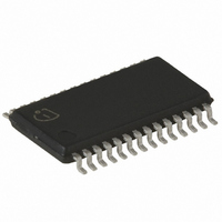
Package Outlines Figure 2-1 Wireless Components P-TSSOP-28-1 package outlines TDA 5211 Product Description P_TSSOP_28.EPS Specification, May 2001 ...
Page 9
Functional Description Contents of this Chapter 3.1 Pin Configuration . . . . . . . . . . . . . . . . . . . . . . . . . . . . . . ...
Page 10
Pin Configuration Figure 3-1 Wireless Components TDA ...
Page 11
Pin Definition and Function In the subsequent table the internal circuits connected to the pins of the device are shown. ESD-protection circuits are omitted to ease reading. . Table 3-1 Pin Definition and Function Pin No. Symbol 1 CRST1 ...
Page 12
TAGC 4 5 AGND 6 LNO 7 VCC MIX 8 10 AGND 11 FSEL Wireless Components 4 . 1 ...
Page 13
IFO DGND 14 VDD 15 MSEL 15 16 CSEL 1 6 Wireless Components 10.7 MHz IF Mixer Output Digital Ground Return 5V Supply ...
Page 14
LIM LIMX SLP SLN OPP 21 Wireless Components ...
Page 15
FFB THRES 3VOUT DATA Wireless Components ...
Page 16
PDO PDWN CRST2 Wireless Components TDA 5211 Functional Description Peak Detector Output ...
Page 17
Functional Block Diagram VCC LNO MI MIX LNI 3 RF LNA TAGC VCC 14 DGND 13 11 2,7 5,10 VCC AGND (FSEL) Figure 3-2 3.4 Functional Blocks 3.4.1 Low Noise Amplifier ...
Page 18
TAGC pin (Pin 4) and should be chosen along with the appropriate threshold voltage according to the intended operat- ing case and interference scenario to be expected during operation. The opti- mum choice ...
Page 19
The calculation of the value of the necessary quartz load capacitance is shown in Section 4.3, the quartz frequency calculation is explained in Section 4.4. 3.4.5 Limiter The Limiter coupled multistage amplifier with a cumulative gain of ...
Page 20
The demodulator circuit is switched off in case of reception of ASK signals. 3.4.7 Data Filter The data filter comprises an OP-Amp with a bandwidth of 100kHz used as a voltage follower and two 100k capacitors a 2nd order Sallen-Key ...
Page 21
Applications Contents of this Chapter 4.1 Choice of LNA Threshold Voltage and Time Constant . . . . . . . . . . . . 4-2 4.2 Data Filter Design . . . . . . . . ...
Page 22
Choice of LNA Threshold Voltage and Time Constant In the following figure the internal circuitry of the LNA automatic gain control is shown. Figure 4-1 The LNA automatic gain control circuitry consists of an operational transimped- ance amplifier that ...
Page 23
Figure 4-2 The switching point should be chosen according to the intended operating sce- nario. The determination of the optimum point is described in the accompanying Application Note, a threshold voltage level ...
Page 24
Data Filter Design Utilising the on-board voltage follower and the two 100k 2nd order Sallen-Key low pass data filter can be constructed by adding 2 exter- nal capacitors between pins 19 (SLP) and 22 (FFB) and to pin 21 ...
Page 25
... Wireless Components C S Input Crystal impedance Z 1-28 Determination of Series Capacitance Value for the Quartz Oscillator the load capacitance (refer to the quartz crystal specification =870 TDA 5211 Applications Pin 28 TDA5211 Pin 1 Quartz_load_5211.wmf 7 Specification, May 2001 ...
Page 26
Quartz Frequency Calculation As described in Section 3.4.3 the operating range of the on-chip VCO is wide enough to guarantee a receive frequency range between 310 and 350MHz. The VCO signal is divided by 2 before applied to the ...
Page 27
Data Slicer Threshold Generation The threshold of the data slicer can be generated using an external R-C inte- grator as shown in Figure 4-5. The cut-off frequency of the R-C integrator has to be lower than the lowest frequency ...
Page 28
... ASK/FSK Switch Functional Description The TDA5211 is containing an ASK/FSK switch which can be controlled via Pin 15 (MSEL). This switch is actually consisting of 2 operational amplifiers that are having a gain case of the ASK amplifier and a gain case of the FSK amplifier in order to achieve an appropriate demodulation gain charac- teristic ...
Page 29
This offset voltage is generated by the bias current of the negative input of the comparator (i.e. 20nA) running over the external resistor R. This voltage raises the voltage appearing at pin 20 (e.g. 1mV with R = 100k ). ...
Page 30
ASK Mode In case the receiver is operated in ASK mode the datapath frequency charac- tersitic is dominated by the data filter alone, thus it is lowpass shaped.The cutoff frequency is determined by the external capacitors C12 and C14 ...
Page 31
... In the powerdown mode the capacitor is only discharged by leakage currents. In order to reduce the turn-on time in the presence of large values pre- charge circuit was included in the TDA5211 as shown in the following figure. Figure 4-10 Wireless Components ...
Page 32
This circuit charges the capacitor C with an inrush current I 220µA for a duration of T equal to the voltage U 2.5V. As soon as these voltages are equal or the duration T precharge circuit is disabled. is the ...
Page 33
Figure 4- example the choice 22nF and C = 47nF yields = 0.44ms 0.71ms 0.53ms 3 This means that in this case the inrush current could flow for a ...
Page 34
Reference Contents of this Chapter 5.1 Electrical Data ...
Page 35
Electrical Data 5.1.1 Absolute Maximum Ratings WARNING The maximum ratings may not be exceeded under any circumstances, not even momentarily and individually, as permanent damage to the IC will result. Table 5-1 Absolute Maximum Ratings, Ambient temperature T # ...
Page 36
Operating Range Within the operational range the IC operates as explained in the circuit descrip- tion. The AC/DC characteristic limits are not guaranteed. Currents flowing into the device are denoted as positive currents and v.v. Supply voltage: VCC = ...
Page 37
AC/DC Characteristics at T AC/DC characteristics involve the spread of values guaranteed within the spe- cified voltage and ambient temperature range. Typical characteristics are the median of the production. Currents flowing into the device are denoted as po- sitive ...
Page 38
Table 5-3 AC/DC Characteristics with T Parameter Symbol 3 Voltage Gain Antenna G AntMI 315 MHz RF 4 Noise Figure NF Signal Input LNI GND, low gain mode THRES 1 Input impedance ...
Page 39
Table 5-3 AC/DC Characteristics with T Parameter Symbol Signal Output IFO (PIN 12) 1 Output impedance Z 2 Conversion Voltage G Gain f = 315 MHz RF 3 Noise Figure, SSB DSB NF+3dB ...
Page 40
Table 5-3 AC/DC Characteristics with T Parameter Symbol PEAK DETECTOR Signal Output PDO (PIN 26) 1 Load current I load 2 Leakage current I leakage CRYSTAL OSCILLATOR Signals CRSTL1, CRISTL 2, (PINS 1/28) 1 Operating frequency f CRSTL 2 Input ...
Page 41
Table 5-3 AC/DC Characteristics with T Parameter Symbol PLL DIVIDER Signal CSEL (PIN 16 range 5.xxMHz V CRSTL CSEL 2 f range V CRSTL CSEL 10.xxMHz 3 Input bias current I CSEL CSEL Measured only in lab. Wireless ...
Page 42
AC/DC Characteristics at T Currents flowing into the device are denoted as positive currents and vice versa. Table 5-4 AC/DC Characteristics with T Parameter Symbol Supply Supply Current 1 Supply current PDWN standby mode 2 Supply current, ...
Page 43
Table 5-4 AC/DC Characteristics with T Parameter Symbol DATA FILTER Slicer, Signal Output DATA (PIN 25) 1 Maximum Datarate DR 2 LOW output voltage V SLIC_L 3 HIGH output voltage V SLIC_H Slicer, Signal Output DATA (PIN 20) 1 Precharge ...
Page 44
Test Circuit The device performance parameters marked with sured on an Infineon evaluation board. This evaluation board can be obtained together with evaluation boards of the accompanying transmitter device TDA5101 in an evaluation kit that may be ordered on ...
Page 45
Test Board Layouts Figure 5-2 Figure 5-3 Wireless Components Top Side of the Evaluation Board Bottom Side of the Evaluation Board TDA 5211 preliminary Reference tda521x_testboard_20_top.WMF tda521x_testboard_20_bot.WMF Specification, May 2001 ...
Page 46
Figure 5-4 Wireless Components Component Placement on the Evaluation Board TDA 5211 preliminary Reference tda521x_testboard_20_plc.EMF Specification, May 2001 ...
Page 47
... Bill of Materials The following components are necessary for evaluation of the TDA5211 at 315 MHz without use of a Microchip HCS512 decoder. Table 5-5 Bill of Materials Ref Value R1 100k R2 100k R3 820k R4 240k R5 360k R6 10k L1 15nH L2 12pF C1 3 10pF C3 6.8pF C4 100pF C5 47nF C6 15nH C7 100pF ...
Page 48
... S4 IC1 TDA 5211 Please note that a capacitor has to be soldered in place L2 and an inductor in place C6. The following components are necessary in addition to the above mentioned ones for evaluation of the TDA5211 in conjunction with a Microchip HCS512 decoder. Table 5-6 Bill of Materials Addendum Ref Value R7 100k ...
Page 49
... Stub Stretchers and a HP8514 network analyser. Maximum gain is shown at point 1 at 18.5 dB, minimum noise figure ist 1.9dB at point 2, step size of circles is 0.5dB. Figure 5-5 Wireless Components Gain and Noise Circles of the TDA5211 at 315 MHz TDA 5211 preliminary Reference Specification, May 2001 ...
Page 50
Wireless Components TDA 5211 preliminary Reference Specification, May 2001 ...
Page 51
... Top Side of the Evaluation Board . . . . . . . . . . . . . . . . . . . . . . . . . . . . . . . . . . . . . . . . . 5-13 Figure 5-3 Bottom Side of the Evaluation Board . . . . . . . . . . . . . . . . . . . . . . . . . . . . . . . . . . . . . . . 5-13 Figure 5-4 Component Placement on the Evaluation Board . . . . . . . . . . . . . . . . . . . . . . . . . . . . . . 5-14 Figure 5-5 Gain and Noise Circles of the TDA5211 at 315 MHz 5-17 Wireless Components List of Figures - 1 TDA 5211 List of Figures 2-3 ...
Page 52
List of Tables Table 3-1 Pin Definition and Function . . . . . . . . . . . . . . . . . . . . . . . . . . . . . . . ...