TDA5211 Infineon Technologies, TDA5211 Datasheet - Page 39
TDA5211
Manufacturer Part Number
TDA5211
Description
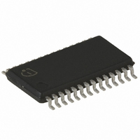
IC FSK/ASK RECEIVER P-TSSOP-28
Manufacturer
Infineon Technologies
Type
Receiverr
Datasheet
1.TDA5211.pdf
(52 pages)
Specifications of TDA5211
Package / Case
28-TSSOP
Frequency
310MHz ~ 350MHz
Sensitivity
-110dBm
Modulation Or Protocol
ASK, FSK
Applications
Alarm Systems, Communication Systems
Current - Receiving
5.7mA
Data Interface
PCB, Surface Mount
Antenna Connector
PCB, Surface Mount
Voltage - Supply
4.5 V ~ 5.5 V
Operating Temperature
-40°C ~ 105°C
Operating Frequency
350 MHz
Operating Supply Voltage
5 V
Maximum Operating Temperature
+ 150 C
Minimum Operating Temperature
- 40 C
Mounting Style
SMD/SMT
Operating Temperature (min)
-40C
Operating Temperature Classification
Automotive
Product Depth (mm)
4.4mm
Product Length (mm)
9.7mm
Operating Supply Voltage (min)
4.5V
Operating Supply Voltage (typ)
5V
Operating Supply Voltage (max)
5.5V
Lead Free Status / RoHS Status
Lead free / RoHS Compliant
Features
-
Memory Size
-
Data Rate - Maximum
-
Lead Free Status / Rohs Status
Compliant
Other names
SP000016390
TDA5211INTR
TDA5211XT
TDA5211XTINTR
TDA5211XTINTR
TDA5211INTR
TDA5211XT
TDA5211XTINTR
TDA5211XTINTR
Available stocks
Company
Part Number
Manufacturer
Quantity
Price

Part Number:
TDA5211
Manufacturer:
INFINEON/英飞凌
Quantity:
20 000
Part Number:
TDA5211B3
Manufacturer:
INFINEON/英飞凌
Quantity:
20 000
Company:
Part Number:
TDA5211B4
Manufacturer:
SIEMENS
Quantity:
5 510
Part Number:
TDA5211B4
Manufacturer:
INFINEON/英飞凌
Quantity:
20 000


Wireless Components
Table 5-3 AC/DC Characteristics with T
Signal Output IFO (PIN 12)
1
2
3
4
LIMITER
Signal Input LIM/X (PINS 17/18)
1
2
3
4
DATA FILTER
1
2
3
SLICER
Signal Output DATA (PIN 25)
1
2
3
Slicer, Signal Output DATA (PIN 20)
1
Parameter
Output impedance
Conversion Voltage
Gain f
Noise Figure, SSB
(
RF to IF isolation
Input Impedance
RSSI dynamic range
RSSI linearity
Operating frequency
(3dB points)
Useable bandwidth
RSSI Level at Data Fil-
ter Output SLP,
RF
RSSI Level at Data Fil-
ter Output SLP,
RF
Maximum Datarate
LOW output voltage
HIGH output voltage
Precharge Current Out
~
DSB NF+3dB)
IN
IN
=-103dBm
=-30dBm
RF
= 315 MHz
Symbol
BW
I
RSSI
V
PCH_SLN
RSSI
DR
LIN
V
DR
NF
A
G
SLIC_H
SLIC_L
Z
Z
f
RF-IF
BB FILT
LIM
IFO
MIX
LIM
RSSI
RSSI
MIX
max
high
low
A
25 °C, V
1.3V
-100
264
min
V
0.3
1.8
60
5
0
S
-
Limit Values
VCC
V
5 - 6
10.7
-220
330
330
S
typ
±
21
13
46
= 4.5 ... 5.5 V (continued)
-1V
1
0.7V
-300
max
396
100
100
V
0.1
80
23
1
3
S
-
kBps
MHz
Unit
kHz
dB
dB
dB
dB
dB
µA
V
V
V
V
Test Conditions
LNA in high gain
mode
LNA in high gain
mode
NRZ, 20pF capaci-
tive loading
see Section 4.7
Specification, May 2001
TDA 5211
Reference
preliminary
L
Item
Related parts for TDA5211
Image
Part Number
Description
Manufacturer
Datasheet
Request
R

Part Number:
Description:
Manufacturer:
Infineon Technologies AG
Datasheet:
Part Number:
Description:
Manufacturer:
Infineon Technologies AG
Datasheet:
Part Number:
Description:
Manufacturer:
Infineon Technologies AG
Datasheet:
Part Number:
Description:
Manufacturer:
Infineon Technologies AG
Datasheet:
Part Number:
Description:
Manufacturer:
Infineon Technologies AG
Datasheet:
Part Number:
Description:
Manufacturer:
Infineon Technologies AG
Datasheet:
Part Number:
Description:
Manufacturer:
Infineon Technologies AG
Datasheet:
Part Number:
Description:
16-bit microcontroller with 2x2 KByte RAM
Manufacturer:
Infineon Technologies AG
Datasheet:
Part Number:
Description:
NPN silicon RF transistor
Manufacturer:
Infineon Technologies AG
Datasheet:
Part Number:
Description:
NPN silicon RF transistor
Manufacturer:
Infineon Technologies AG
Datasheet:
Part Number:
Description:
NPN silicon RF transistor
Manufacturer:
Infineon Technologies AG
Datasheet:
Part Number:
Description:
NPN silicon RF transistor
Manufacturer:
Infineon Technologies AG
Datasheet:
Part Number:
Description:
Si-MMIC-amplifier in SIEGET 25-technologie
Manufacturer:
Infineon Technologies AG
Datasheet:
Part Number:
Description:
IGBT Power Module
Manufacturer:
Infineon Technologies AG
Datasheet:
Part Number:
Description:
IC for switching-mode power supplies
Manufacturer:
Infineon Technologies AG
Datasheet: