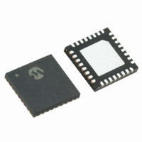
MRF89XA-I/MQ Microchip Technology, MRF89XA-I/MQ Datasheet - Page 18

MRF89XA-I/MQ
Manufacturer Part Number
MRF89XA-I/MQ
Description
TXRX ISM SUB-GHZ ULP 32QFN
Manufacturer
Microchip Technology
Specifications of MRF89XA-I/MQ
Package / Case
32-WFQFN Exposed Pad
Frequency
863MHz ~ 870MHz, 902MHz ~ 928MHz, 950MHz ~ 960MHz
Data Rate - Maximum
200kbps
Modulation Or Protocol
FSK, OOK
Applications
ISM
Power - Output
12.5dBm
Sensitivity
-113dBm
Voltage - Supply
2.1 V ~ 3.6 V
Current - Receiving
3mA
Current - Transmitting
25mA
Data Interface
PCB, Surface Mount
Antenna Connector
PCB, Surface Mount
Operating Temperature
-40°C ~ 85°C
Number Of Receivers
1
Number Of Transmitters
1
Wireless Frequency
863 MHz to 870 MHz, 902 MHz to 928 MHz, 950 MHz to 960 MHz
Interface Type
SPI
Noise Figure
- 112 dBc
Output Power
- 8.5 dBm, + 12.5 dBm
Operating Supply Voltage
2.1 V to 3.6 V
Maximum Operating Temperature
+ 85 C
Mounting Style
SMD/SMT
Maximum Data Rate
256 Kbps
Maximum Supply Current
25 mA
Minimum Operating Temperature
- 40 C
Modulation
FSK
Lead Free Status / RoHS Status
Lead free / RoHS Compliant
Memory Size
-
Lead Free Status / Rohs Status
Lead free / RoHS Compliant
Available stocks
Company
Part Number
Manufacturer
Quantity
Price
Company:
Part Number:
MRF89XA-I/MQ
Manufacturer:
MICROCHIP
Quantity:
12 000
2.6
This section summarizes the settings for each
operating mode of the MRF89XA to save power, based
on the operations and available functionality. The
timing requirements for switching between modes
described in Section 5.3 “Switching Times and
Procedures”.
TABLE 2-3:
TABLE 2-4:
DS70622B-page 18
MRF89XA
Sleep
Stand-by
FS
Receive
Transmit
CSCON
CSDAT
SDO
SDI
SCK
IRQ0
IRQ1
DATA
CLKOUT
PLOCK
Note 1:
Chip.Mode
Mode
Pin
2:
3:
MRF89XA Operating Modes
(Includes Power-Saving Mode)
High-Z if Continuous mode is activated; otherwise, Output.
Output if PLL_lock_en = 1; otherwise, High-Z.
Valid logic states must be applied to inputs at all times to avoid unwanted leakage currents.
(GCONREG<7:5>
CMOD<2:0> bits
High-Z
High-Z
High-Z
High-Z
Sleep
Mode
Input
Input
Input
Input
Input
Input
OPERATING MODES
PIN CONFIGURATION VS. CHIP MODE
000
001
010
011
100
Stand-by
Output
Output
Output
Output
Mode
Input
Input
Input
Input
Input
Input
(1)
(1)
(2)
SPI, POR.
SPI, POR, Top regulator, digital regulator, XO, CLKOUT (if activated through
CLKOREG).
Same as Stand-by + VCO regulator, all PLL and LO generation blocks.
Same as FS mode + LNA, first mixer, IF amplifier, second mixer set, channel filters,
baseband amplifiers and limiters, RSSI, OOK or FSK demodulator, BitSync and all
digital features if enabled.
Same as FS mode + DDS, Interpolation filters, all up-conversion mixers, PA driver,
PA and external PARS pin (pin 29) output for the PA choke.
FS Mode
Output
Output
Output
Output
Input
Input
Input
Input
Input
Input
(1)
(1)
(2)
Output
Receive
Output
Output
Output
Output
Mode
Input
Input
Input
Input
Input
Preliminary
(2)
Transmit
Output
Output
Output
Output
Mode
Input
Input
Input
Input
Input
Input
2.6.1
Table 2-3 lists the different operating modes of the
MRF89XA, which can be used to save power.
2.6.2
Table 2-4 lists the state of the digital I/Os in each of the
above described modes of operation, regardless of the
data operating mode (Continuous, Buffered, or
Packet).
(2)
Active Blocks
CSCON has priority over CSDAT.
Output only if CSCON or CSDAT = 0.
MODES OF OPERATION
DIGITAL PIN CONFIGURATION VS.
CHIP MODE
© 2010 Microchip Technology Inc.
Comment


