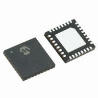
MRF89XA-I/MQ Microchip Technology, MRF89XA-I/MQ Datasheet - Page 78

MRF89XA-I/MQ
Manufacturer Part Number
MRF89XA-I/MQ
Description
TXRX ISM SUB-GHZ ULP 32QFN
Manufacturer
Microchip Technology
Specifications of MRF89XA-I/MQ
Package / Case
32-WFQFN Exposed Pad
Frequency
863MHz ~ 870MHz, 902MHz ~ 928MHz, 950MHz ~ 960MHz
Data Rate - Maximum
200kbps
Modulation Or Protocol
FSK, OOK
Applications
ISM
Power - Output
12.5dBm
Sensitivity
-113dBm
Voltage - Supply
2.1 V ~ 3.6 V
Current - Receiving
3mA
Current - Transmitting
25mA
Data Interface
PCB, Surface Mount
Antenna Connector
PCB, Surface Mount
Operating Temperature
-40°C ~ 85°C
Number Of Receivers
1
Number Of Transmitters
1
Wireless Frequency
863 MHz to 870 MHz, 902 MHz to 928 MHz, 950 MHz to 960 MHz
Interface Type
SPI
Noise Figure
- 112 dBc
Output Power
- 8.5 dBm, + 12.5 dBm
Operating Supply Voltage
2.1 V to 3.6 V
Maximum Operating Temperature
+ 85 C
Mounting Style
SMD/SMT
Maximum Data Rate
256 Kbps
Maximum Supply Current
25 mA
Minimum Operating Temperature
- 40 C
Modulation
FSK
Lead Free Status / RoHS Status
Lead free / RoHS Compliant
Memory Size
-
Lead Free Status / Rohs Status
Lead free / RoHS Compliant
Available stocks
Company
Part Number
Manufacturer
Quantity
Price
Company:
Part Number:
MRF89XA-I/MQ
Manufacturer:
MICROCHIP
Quantity:
12 000
3.9
In Continuous mode, the NRZ data to/from the
modulator/demodulator is accessed by the host
microcontroller on the bidirectional DATA pin (pin 20).
The SPI Data, FIFO, and packet handler are therefore
inactive. Figure 3-17 illustrates the Continuous mode
of operation.
FIGURE 3-17:
FIGURE 3-18:
3.9.1
In TX mode, a synchronous data clock for a host
microcontroller is provided on the IRQ1 pin (pin 22). Its
timing with respect to the data is illustrated in
Figure 3-18. DATA is internally sampled on the rising
edge of DCLK so the microcontroller can change the
logic state anytime outside the setup/hold time zone.
The setup and hold times are shown in gray in the
Figure 3-18.
The use of DCLK is compulsory in FSK and optional in
OOK.
DS70622B-page 78
MRF89XA
DATA (NRZ)
Continuous Mode
Data
TX PROCESSING
DCLK
Datapath
TX/RX
RX
Recognition
CONTINUOUS MODE BLOCK DIAGRAM
TX PROCESSING IN CONTINUOUS MODE
SYNC
T_DATA
MRF89XA
T_DATA
Preliminary
Control
3.9.2
If the bit synchronizer is disabled, the raw demodulator
output is made directly available on the DATA pin and
no DCLK signal is provided.
Conversely, if the bit synchronizer is enabled, synchro-
nous cleaned data and clock are made available
respectively on the DATA and IRQ1 pins (pin 20 and
22). DATA is sampled on the rising edge of DCLK and
updated on the falling edge as shown in Figure 3-19.
RX PROCESSING
CONFIG
SPI
© 2010 Microchip Technology Inc.
CSCON
SDO
SCK
SDI
IRQ0
IRQ1 (DCLK)
DATA


