CYRF69213-40LFXC Cypress Semiconductor Corp, CYRF69213-40LFXC Datasheet
CYRF69213-40LFXC
Specifications of CYRF69213-40LFXC
Available stocks


Related parts for CYRF69213-40LFXC

CYRF69213-40LFXC Summary of contents
Page 1
... Pb-Free 40-Pin QFN Package ■ Advanced Development Tools Based on Cypress’s PSoC Tools 1ohm 1-2 uF 470 nF R adio F unction P 1.5 1 1.3/ • 198 Champion Court • San Jose CYRF69213 R F bias 470 95134-1709 • 408-943-2600 Revised February 13, 2009 ® [+] Feedback ...
Page 2
... Applications The CYRF69213 PRoC LP Low Speed is targeted for the following applications: ■ USB Bridge for Human Interface Devices (HID) ❐ Wireless mice ❐ Wireless keyboards ❐ Remote controls ❐ Gaming applications ■ USB Bridge for General Purpose Applications ❐ Consumer electronics ❐ ...
Page 3
... Interrupt output, configure high/low or GPIO 28 P1.5 / MOSI Master Out Slave In Document #: 001-07552 Rev. *D Corner tabs P0 CYRF69213 WirelessUSB LP P0 BAT1 P2 BAT2 * E-PAD Bottom Side 10 BIAS Function CYRF69213 30 XOUT / GPIO 29 MISO / GPIO 28 P1.5 / MOSI 27 IRQ / GPIO 26 P1.4 / SCK REG_MICRO 23 V DD_Micro Page [+] Feedback ...
Page 4
... In addition, the MCU function includes a Watchdog timer, a vectored interrupt controller, a 16-bit Free-Running Timer, and 12-bit Programmable Interrupt Timer. The MCU function supports in-system programming by using the D+ and D– pins as the serial programming mode interface. The programming protocol is not USB. CYRF69213 Page [+] Feedback ...
Page 5
... Sets the number of consecutive symbols for non correlation to detect end of packet. PREAMBLE_ADR 0xAAAA09 AAAA are the two preamble bytes. Any other byte can also be written into the preamble register file. The number of preamble bytes to be sent should be >8. Document #: 001-07552 Rev. *D CYRF69213 DESCRIPTION DESCRIPTION Page [+] Feedback ...
Page 6
... Lower data rates typically provide longer range and/or a more +4 robust link. 0 Link Layer Modes –5 The CYRF69213 IC device supports the following data packet –10 framing features: –15 SOP – Packets begin with a 2-symbol Start of Packet (SOP) –20 marker. This is required in GFSK and 8DR modes, but is optional in DDR mode and is not supported in SDR mode ...
Page 7
... The CYRF69213 IC supports packet length bytes; interrupts are provided to allow an MCU to use the transmit and receive buffers as FIFOs. When transmitting a packet longer than 16 bytes, the MCU can load 16 bytes initially, and add further bytes to the transmit buffer as transmission of data creates space in the buffer ...
Page 8
... The RSSI register returns the relative signal strength of the on-channel signal power. When receiving, the device may be configured to automatically measure and store the relative strength of the signal being received as a 5-bit value. When enabled, an RSSI reading is CYRF69213 0.047µF 0.047µF 0.047µF 0.047µF 0.047µ ...
Page 9
... MCU function and radio function should be connected with a regulated voltage of 3.3V (by setting [bit4] of Registers P13CR, P14CR, P15CR, and P16CR of the MCU function) and the internal 3.3V regulator of the MCU function should be turned on. CYRF69213 Radio Function P1.5/MOSI MOSI MISO P1.4/SCK SCK P1 ...
Page 10
... The user cannot manipulate the Supervisory State status bit [3]. The flags are affected by arithmetic, logic, and shift opera- tions. The manner in which each flag is changed is dependent upon the instruction being executed (for example, AND, OR, XOR). See Table 21. CYRF69213 Byte 1+N Page [+] Feedback ...
Page 11
... Read/Write – – Default 0 0 Bits 7:0 CPU Accumulator [7:0] 8-bit data value holds the result of any logical/arithmetic instruction that uses a source addressing mod Document #: 001-07552 Rev XIO Super – R – – – CYRF69213 Carry Zero Global – – – Page [+] Feedback ...
Page 12
... Document #: 001-07552 Rev [7:0] – – – Stack Pointer [7:0] – – – – – – – – – CYRF69213 – – – – – – – – – – – – Page [+] Feedback ...
Page 13
... The ;Accumulator is unchanged. MOV REG[8], A ;In this case, the Accumula- ;tor is moved to the regis- ;ter space location at ;address 8. The Accumulator ;is unchanged. CYRF69213 Page [+] Feedback ...
Page 14
... Table 18. Destination Direct Source Direct Operand 2 Opcode Immediate Value Instruction Example MOV [7], [8] ;In this case, the value in the CYRF69213 Operand 1 Operand 2 Destination Index Immediate Value 5 ;In this case, the value in ;the memory location at ;address X+7 is added with ...
Page 15
... Opcode Operand 1 Instruction Destination Address Address Example MVI [8], A ;In this case, the value in ;the memory location at ;address indirect ;address. The Accumulator is ;moved into the memory loca- ;tion pointed to by the indi- ;rect address. The indirect ;address is then incremented. CYRF69213 Page [+] Feedback ...
Page 16
... MOV A, expr MOV A, [expr MOV A, [X+expr MOV [expr MOV [X+expr MOV [expr], expr MOV [X+expr], expr MOV X, expr MOV X, [expr MOV X, [X+expr] CYRF69213 Instruction Format Flags MOV [expr MOV MOV MOV A, reg[expr MOV A, reg[X+expr MOV [expr], [expr MOV reg[expr MOV reg[X+expr ...
Page 17
... Free Running Timer Wrap 0x0048 INT2 0x004C Reserved 0x0050 GPIO Port 2 0x0054 Reserved 0x0058 Reserved 0x005C Reserved 0x0060 Reserved 0x0064 Sleep Timer 0x0068 Program Memory begins here (if below interrupts not used, program memory can start lower) 0x1FFF 8 KB ends here CYRF69213 Page [+] Feedback ...
Page 18
... CYRF69213 device enables this type of in-system programming by using the D+ and D– pins as the serial programming mode interface. This allows an external controller to cause the CYRF69213 part to enter serial programming mode and then to use the test queue to issue Flash access functions in the SROM. The programming protocol is not USB. ...
Page 19
... SSC instruction with an accumulator value of 00h. The SWBootReset function does not execute when the SSC instruction is executed with a bad key value and a nonzero function code. A CYRF69213 device executes the HALT instruction if a bad value is given for either KEY1 or KEY2. 0,F8h ...
Page 20
... DELAY 0,FEh For a CPU speed of 12 MHz set to 56h Document #: 001-07552 Rev. *D ProtectBlock Function The CYRF69213 device offers Flash protection on a block-by-block basis. Table 29 lists the protection modes available. In the table, ER and EW are used to indicate the ability to perform external reads and writes. For internal writes used ...
Page 21
... Stack Pointer value when SSC is executed BLOCKID 0,FAh Table number to read The table space for the CYRF69213 is simply a 64-byte row broken up into eight tables of eight bytes. The tables are Document #: 001-07552 Rev. *D numbered zero through seven. All user and hidden blocks in the CYRF69213 parts consist of 64 bytes ...
Page 22
... ID pointer to data buffer Clock ClockW ClockE multiplier flash macro sequence delay count temporary result code ; create 3 byte stack frame (2 + pushed A) ; save stack frame for supervisory code ;FLASH_OPER_KEY - 3Ah CYRF69213 F8h F8h F8h Figure 8. Table 23 Page [+] Feedback ...
Page 23
... The internal low speed oscillator of nominally 32 KHz provides a slow clock source for the CYRF69213 in suspend mode, particularly to generate a periodic wakeup interrupt and also to provide a clock to sequential logic during power up and power down events when the main clock is stopped ...
Page 24
... CLK_EXT CLK_24MHz Clock Architecture Description The CYRF69213 clock selection circuitry allows the selection of independent clocks for the CPU, USB, Interval Timers, and Capture Timers. The CPU clock, CPUCLK, can be sourced from the external crystal oscillator or the Internal 24 MHz Oscillator. The selected ...
Page 25
... These bits are used to trim the frequency of the low power oscillator Document #: 001-07552 Rev. *D ■ Internal 32 kHz Low power Oscillator except when in sleep mode ■ CPUCLK after the programmable divider R/W R/W R kHz Bias Trim [1:0] 32 kHz Freq Trim [3:0] R/W R/W R CYRF69213 Gain[4:0] R/W R/W R R/W R/W R Page [+] Feedback ...
Page 26
... CPU CLK Select 0 = Internal 24 MHz Oscillator 1 = External clock—External clock at CLKIN (P0.0) pin Note The CPU speed selection is configured using the OSC_CR0 Register Document #: 001-07552 Rev USB CLK Reserved Select R/W – – Table 38) (Table 37) CYRF69213 CPUCLK Se- lect – – R Page [+] Feedback ...
Page 27
... Bits 2:0 CPU Speed [2:0] The CYRF69213 may operate over a range of CPU clock speeds. The reset value for the CPU Speed bits is zero; therefore, the default CPU speed is one-eighth of the internal 24 MHz MHz Regardless of the CPU Speed bit’s setting, if the actual CPU speed is greater than 12 MHz, the 24 MHz operating requirements apply. An example of this scenario is a device that is configured to use an external clock, which is sup- plying a frequency of 20 MHz. If the CPU speed register’ ...
Page 28
... Internal 32 kHz Low pow TCAPCLK Document #: 001-07552 Rev Reserved – – – TCAPCLK Select ITMRCLK Divider R/W R/W R Oscillator. However this configuration is not used in sleep mode. CYRF69213 Fine Tune USB Osclock Only Disable – R/W R ITMRCLK Select R/W R/W R Page [+] Feedback ...
Page 29
... The programmable interval timer generates an interrupt to the CPU on each reload. The parameters to be set appears on the device editor view of PSoC Designer after you place the CYRF69213 Timer User Module. The parameters ...
Page 30
... The internal clocking mode is active after a reset, until changed by user firmware. Note The CPU clock defaults to 3 MHz (Internal 24 MHz Oscil- lator divide-by-8 mode) at POR to guarantee operation at the low V that might be present during the supply ramp. CC CYRF69213 Capture1 Int CLKOUT Select - ...
Page 31
... Read/Write 0 0 Default he bits of the CPU_SCR register are used to convey status and control of events for various functions of an CYRF69213 device T Bit 7 GIES The Global Interrupt Enable Status bit is a read only status bit and its use is discouraged. The GIES bit is a legacy bit, which was used to provide the ability to read the GIE bit of the CPU_F register ...
Page 32
... Firmware sets the SLEEP bit in the CPU_SCR0 register. The Bus Request (BRQ) signal to the CPU is immediately asserted. This is a request by the system to halt CPU operation at an instruction boundary. The CPU samples BRQ on the positive edge of CPUCLK. CYRF69213 (Table 37). When the sleep time 2 1 ...
Page 33
... To avoid current consumption make sure ITMRCLK, TCPCLK, and USBCLK are not sourced by either low power 32KHz oscillator or 24 MHz crystal-less oscillator. All the other blocks go to the power down mode automatically on suspend. CYRF69213 On the falling edge of is halted; the Flash and Figure 13 Page ...
Page 34
... CLK32K INT SLEEP PD BANDGAP LVD PPOR ENABLE SAMPLE SAMPLE LVD/POR CPUCLK/ (Not to Scale) 24MHz BRQ BRA CPU Document #: 001-07552 Rev. *D Figure 13. Wakeup Timing Interrupt is double sampled by 32K clock and PD is negated to system CYRF69213 CPU is restarted after 90 ms (nominal) Page [+] Feedback ...
Page 35
... PORLEV[1: precision-power-on-reset event precision-power-on-reset event has tripped Document #: 001-07552 Rev PORLEV[1:0] Reserved R/W R/W – Max. Reserved Reserved Reserved Reserved 4.528 4.689 4.774 Reserved – – – Table 43) CYRF69213 VM[2:0] R/W R/W R (Table 44 LVD PPOR – Page [+] Feedback ...
Page 36
... P0.7 Data Bits 6:5 Reserved The use of the pins as the P0.6–P0.5 GPIOs and the alternative functions exist in the CYRF69213 Bits 4:3 P0.4–P0.3 Data/INT2 – INT1 In addition to their use as the P0.4–P0.3 GPIOs, these pins can also be used for the alternative functions as the Inter- rupt pins (INT0– ...
Page 37
... In addition to their use as the P1.6–P1.3 GPIOs, these pins can also be used for the alternative function as the SPI interface pins. To configure the P1.6–P1.3 pins, refer to the P1.3–P1.6 Configuration Register The use of the pins as the P1.6–P1.3 GPIOs and the alternative functions exist in all the CYRF69213 parts Bit 2 P1 ...
Page 38
... R/W R/W Default 0 0 This register is used to configure P0.1 In the CYRF69213, only 8 mA sink drive capability is available on this pin regardless of the setting of the High Sink bit Bit 7: Reserved Document #: 001-07552 Rev enable the pin for GPIO, clear the corresponding VREG Output or SPI Use bit. The SPI function controls the output ...
Page 39
... P0.3–P0.4, respectively. These pins are shared between the P0.3–P0.4 GPIOs and T the INT0–INT2. These registers exist in all CYRF69213 parts. The INT0–INT2 interrupts are different than all the other GPIO interrupts. These pins are connected directly to the interrupt controller to provide three edge-sensitive interrupts with independent interrupt vectors ...
Page 40
... Reserved R/W – – for information on enabling USB. When USB is enabled, none of the controls in this (Table 52 Int Act Low TTL Thresh- Reserved old R/W R/W – CYRF69213 Open Drain Reserved Output En- able R/W – R OL3 Open Drain Pull up En- Output En- able ...
Page 41
... This register controls the operation of the P1.3 pin. This register exists in all CYRF69213 parts The P1.3 GPIO’s threshold is always set to TTL When the SPI hardware is enabled, the output enable and output state of the pin is controlled by the SPI circuitry. When the SPI hardware is disabled, the pin is controlled by the Output Enable bit and the corresponding bit in the P1 data register Regardless of whether the pin is used as an SPI or GPIO pin the Int Enable, Int act Low, 3 ...
Page 42
... High Sink bit GPIO Configurations for Low Power Mode: To ensure low power mode, unbonded GPIO pins in CYRF69213 must be placed in a non floating state. The following assembly code snippet shows how this is achieved. This snippet can be added as a part of the initialization routine. ...
Page 43
... SCK Clock Generation SCK Clock Select SCK Clock Phase/Polarity Select SCK Output Shift Buffer Master/Slave Set SCK Shift Buffer LE_SEL Input Shift Buffer SCK_OE SS_N_OE MISO_OE MOSI_OE CYRF69213 SCK_OE SCK GPIO Block SS_N SS_N SS_N_OE MISO_OE MISO/MOSI MISO Crossbar MOSI_OE MOSI Page [+] Feedback ...
Page 44
... Master mode, pin P1.4 must be configured as an output; for SPI Slave mode, pin P1.4 must be configured as an input Document #: 001-07552 Rev SPIData[7:0] R/W R/W R Comm Mode CPOL R/W R/W R 56), the input/output direction of pins P1.3, P1.5, and P1.6 is set automatically by CYRF69213 R/W R/W R CPHA SCLK Select R/W R/W R Table 61 shows the timing for the var- Page ...
Page 45
... SCLK SSEL DAT SCLK SSEL DAT SSEL DAT A Document #: 001-07552 Rev. *D Diagram LSB Bit 2 Bit 3 Bit 4 Bit 5 X LSB Bit 2 Bit 3 Bit 4 Bit 5 X LSB Bit 2 Bit 3 Bit 4 Bit 5 CYRF69213 Bit 6 Bit 7 MSB X Bit 6 Bit 7 MSB X Bit 6 Bit 7 MSB Page [+] Feedback ...
Page 46
... KHz 11 96 125 KHz Timer Registers All timer functions of the CYRF69213 are provided by a single timer block. The timer block is asynchronous from the CPU clock. Figure 16. 16-Bit Free-Running Counter Block Diagram Tim er C apture C lock Table 63. Free-Running Timer Low Order Byte (FRTMRL) [0x20] [R/W] ...
Page 47
... This register holds the higher 4 bits of the timer. While writing into the 12-bit reload register, write lower byte first then the higher nibble Document #: 001-07552 Rev Prog Interval Timer [7: Prog Interval Timer [11:8] – – Prog Interval [7:0] R/W R/W R – – R CYRF69213 R/W R/W R Prog Interval[11:8] R/W R/W R Page [+] Feedback ...
Page 48
... ACBE ACBF ACC0 running counter Figure 18. Memory Mapped Registers Read/Write Timing Diagram clk_sys rd_wrn Valid Addr rdata wdata Document #: 001-07552 Rev. *D 12-bit programmable timer load timing 16-bit free running counter loading timing Memory mapped registers Read/Write timing diagram CYRF69213 Page [+] Feedback ...
Page 49
... It simply prevents a posted interrupt from becoming pending. Nested interrupts can be accomplished by re-enabling interrupts inside an interrupt service routine this, set the IE bit in the Flag Register. A block diagram of the CYRF69213 Interrupt Controller is shown in Figure 19. Figure 19. Interrupt Controller Block Diagram ...
Page 50
... When an INT_CLRx register is read, any bits that are set indicates an interrupt has been posted for that hardware resource. Therefore, reading these registers gives the user the ability to determine all posted interrupts INT1 GPIO Port 0 SPI Receive SPI Transmit R/W R/W R CYRF69213 INT0 POR/LVD R/W R/W R Page [+] Feedback ...
Page 51
... Software interrupts can aid in debugging interrupt service routines by eliminating the need to create system level interac- tions that are sometimes necessary to create a hardware-only interrupt Reserved – – – CYRF69213 USB EP2 USB EP1 USB EP0 R/W R/W R ...
Page 52
... GPIO Port 2 Reserved Int Enable R/W R/W R Timer USB Active USB Reset Int Enable Int Enable Int Enable R/W R/W R CYRF69213 INT2 16-bit Reserved Int Enable Counter Wrap Int Enable R/W R/W R USB EP2 USB EP1 USB EP0 Int Enable Int Enable ...
Page 53
... Writing to this register clears all pending interrupts Document #: 001-07552 Rev INT1 GPIO Port 0 SPI Receive Int Enable Int Enable Int Enable R/W R/W R Pending Interrupt [7:0] R/W R/W R CYRF69213 SPI Transmit INT0 POR/LVD Int Enable Int Enable Int Enable R/W R/W R R/W R/W R Page [+] Feedback ...
Page 54
... Document #: 001-07552 Rev Reserved – – – VREG is not enabled or to the internally generated CC Table 47 for more information Reserved – – – below 4.35V—although no damage or irregularities CC CYRF69213 USB Force State – – R Keep Alive VREG En- able – R/W R Page [+] Feedback ...
Page 55
... Firmware is required to handle the rest of the USB interface with the following tasks: ■ Coordinate enumeration by decoding USB device requests ■ Fill and empty the FIFOs ■ Suspend/Resume coordination ■ Verify and select Data toggle values Device Address[6:0] R/W R/W R CYRF69213 R/W R/W R Page [+] Feedback ...
Page 56
... For Endpoint 0 Count Register, whenever the count updates from a SETUP or OUT transaction, the count register locks and cannot be written by the CPU. Reading the register unlocks it. This prevents firmware from overwriting a status update on it Document #: 001-07552 Rev Reserved R/W R/W R CYRF69213 Byte Count[3:0] R/W R/W R Page [+] Feedback ...
Page 57
... When the SIE writes to these registers they are locked and the processor cannot write to them until after it has read them. Writing to this register clears the upper four bits regardless of the value written OUT Re- ACK’d Trans ceived R/C[3] R/C[3] R CYRF69213 Mode[3:0] R/W R/W R Page [+] Feedback ...
Page 58
... Bit 5 NAK Int Enable This bit, when set, causes an endpoint interrupt to be generated even when a transfer completes with a NAK. Unlike enCoRe, CYRF69213 family members do not generate an endpoint interrupt under these conditions unless this bit is set 0 = Disable interrupt on NAK’d transactions 1 = Enable interrupt on NAK’d transaction Bit 4 ACK’ ...
Page 59
... The Endpoint 2 buffer is comprised of 8 bytes located at address 0x60 to 0x67 Document #: 001-07552 Rev Endpoint 1 Data Buffer [7:0] R/W R/W R/W Unknown Unknown Unknown Endpoint 2 Data Buffer [7:0] R/W R/W R/W Unknown Unknown Unknown CYRF69213 R/W R/W R/W Unknown Unknown Unknown R/W R/W R/W Unknown Unknown Unknown Page [+] Feedback ...
Page 60
... SIE responds with an ACK. If any of the above conditions is not met, the SIE responds with either a STALL or Ignore. A 'TX Count' entry in the IN column means that the SIE transmits the number of bytes specified in the Byte Count Bit [3:0] of the Endpoint Count Register CYRF69213 Comments (Table 81) in response to any IN token. Page ...
Page 61
... ACK 1 1 0001 update 1 STALL 0011 STALL 0011 STALL 0011 ACK ACK 1 1 0001 update CYRF69213 EP0 Interrupt Comments Ignore All junk Ignore junk Ignore update data Yes ACK SETUP Stall IN Ignore Ignore Stall OUT junk Ignore junk Ignore update data ...
Page 62
... ACK 1 1000 update 1 STALL NAK SIE EP0 Mode Register EP0 Count Register MODE DTOG DVAL COUNT FIFO TX 1 1100 STALL NAK CYRF69213 EP0 Interrupt Comments Yes Host ACK'd junk Ignore junk Ignore update data Yes Good OUT junk Ignore junk Ignore ...
Page 63
... Byte Count[3:0] Reserved Byte Count[3:0] Reserved Byte Count[3:0] Mode[3:0] Ack’d trans Mode[3:0] Enable Ack’d trans Mode[3:0] Enable Endpoint 0 Data Buffer [7:0] Endpoint 1 Data Buffer [7:0] CYRF69213 1 0 R/W Default P0.1 Reserved b--bbb-- 00000000 P1.0/D+ bbbbbbbb 00000000 P2.1–P2.0 bbbbbbbb ...
Page 64
... Program Counter [15:8] Stack Pointer [7:0] XOI Super Carry WDRS PORS Sleep Reserved Reserved Sleep Timer [1:0] CPU Speed [2:0] PORLEV[1:0] Reserved VM[2:0] Reserved Reserved CYRF69213 1 0 R/W Default bbbbbbbb ???????? VREG ------bb 00000000 Enable USB Force b------b 00000000 State INT0 POR/LVD bbbbbbbb ...
Page 65
... RSVD RSVD RSVD ABORT EN RSVD RSVD AUTO_CAL_TIME_MAX AUTO_CAL_OFFSET_MINUS_4 RSVD RSVD RSVD RSVD TX Buffer File RX Buffer File SOP Code File Data Code File Preamble File MFG ID File CYRF69213 [ Default -1001000 -bbbbbbb 00000000 bbbbbbbb TXC TXE 00000011 bbbbbbbb IRQEN IRQEN IRQEN --000101 --bbbbbb ...
Page 66
... No GPIO loading, 6 MHz Internal and External Oscillators, Bandgap, Flash, CPU Clock, Timer Clock, USB Clock all disabled 15K ± 5% Ohm enabled UP to inputs through a series resistor limiting input current to 1 mA. AC timing not guaranteed. CYRF69213 [11] .......................... >2000V [11] ................................ 1100V Min. Typ. Max. Unit 2.4 3 ...
Page 67
... CC When regulator is disabled with ‘keep alive’ enable V > 4.35V, 0 < temp < 40° < I < 125 mA VREG V > 4.35V, 0 < temp < 40° < I < VREG Keep Alive bit set in VREGCR CYRF69213 Min. Typ. Max. Unit 0.2 V 0.8 2 –10 10 µ ...
Page 68
... MHz 100 kHz ResBW 100 kHz ResBW 100 kHz ResBW seven steps, monotonic PN Code Pattern 10101010 PN Code Pattern 11110000 >0 dBm –6 dBc, 100 kHz ResBW CYRF69213 Min. Typ. Max. Unit 2.400 2.497 GHz –97 dBm –93 dBm –80 –87 dBm – ...
Page 69
... OUTPUT INCLUDING JIG AND Typical SCOPE V Unit CC 90% Ω 10% Ω GND Ω Rise time: 1 V/ns V THÉVENIN EQUIVALENT Equivalent to OUTPUT CYRF69213 Min. Typ. Max. Unit –47 dBm –43 dBm –48 dBm –59 dBm 0.7 1.3 ms 0.6 ms 270 µs 180 µs 100 µ ...
Page 70
... SCK to data valid –25 Time before leading SCK edge 100 SCK to data valid Time after SS LOW to data valid Before first SCK edge 150 After last SCK edge 150 CYRF69213 Typical Max Unit 25.2 MHz 24.36 MHz 37.12 KHz 47.36 KHz ...
Page 71
... In Master mode first bit is available 0.5 SPICLK cycle before Master clock edge available on the SCLK pin. Document #: 001-07552 Rev. *D Figure 21. Clock Timing T CYC Figure 22. USB Data Signal Timing 90% 90% 10% 10% Figure 23. Clock Timing T CYC Figure 24. USB Data Signal Timing 90% 90% 10% 10% CYRF69213 Page [+] Feedback ...
Page 72
... Paired Transitions PERIOD JR2 Crossover Point Extended Point Diff. Data to SE0 Skew + T PERIOD DEOP Figure 27. Differential Data Jitter Crossover Points Consecutive Transitions PERIOD xJR1 Paired Transitions PERIOD xJR2 CYRF69213 T JR2 Source EOP Width: T EOPT Receiver EOP Width EOPR1 EOPR2 Page [+] Feedback ...
Page 73
... MOSI T T SDO MISO Document #: 001-07552 Rev. *D Figure 28. SPI Master Timing, CPHA = 1 (SS is under firmware control in SPI Master mode) T SCKL MSB T MHD Figure 29. SPI Slave Timing, CPHA = 1 T SCKL MSB T SSU SHD MSB CYRF69213 LSB LSB T SSH LSB LSB Page [+] Feedback ...
Page 74
... MSB MOSI T T SSU SHD T SDO1 MISO MSB Document #: 001-07552 Rev. *D Figure 30. SPI Master Timing, CPHA = 0 (SS is under firmware control in SPI Master mode) T SCKL T MDO Figure 31. SPI Slave Timing, CPHA = 0 T SCKL T SDO CYRF69213 LSB LSB T SSH LSB LSB Page [+] Feedback ...
Page 75
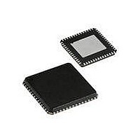
... Table 89. Ordering Information Package 40-pin Pb-Free QFN 6x6 mm Package Diagram Document #: 001-07552 Rev. *D Ordering Part Number CYRF69213-40 LFXC Figure 32. 40-Pin Pb-Free QFN 6x6 mm CYRF69213 001-12917 *A Page [+] Feedback ...
Page 76
... Document History Page Document Title: CYRF69213 Programmable Radio on Chip Low Power Document #: 001-07552 Orig. of Submission REV. ECN No. Change Date ** 436355 OYR See ECN *A 501280 OYR See ECN *B 631538 BOO See ECN *C 2447906 VNY/VGT/ See ECN AESA *D 2661527 TGE/PYRS 18/02/09 Document #: 001-07552 Rev. *D Description of Change New advance data sheet ...
Page 77
... All products and company names mentioned in this document may be the trademarks of their respective holders. PSoC Solutions General psoc.cypress.com Low Power/Low Voltage clocks.cypress.com Precision Analog LCD Drive CAN 2.0b image.cypress.com USB Revised February 13, 2009 CYRF69213 psoc.cypress.com/solutions psoc.cypress.com/low-power psoc.cypress.com/precision-analog psoc.cypress.com/lcd-drive psoc.cypress.com/can psoc.cypress.com/usb Page [+] Feedback ...