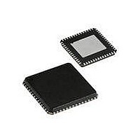
CYRF69213-40LFXC Cypress Semiconductor Corp, CYRF69213-40LFXC Datasheet - Page 20

CYRF69213-40LFXC
Manufacturer Part Number
CYRF69213-40LFXC
Description
IC PROC 8K FLASH 40VQFN
Manufacturer
Cypress Semiconductor Corp
Series
CYRFr
Type
Transceiverr
Datasheet
1.CYRF69213-40LFXC.pdf
(77 pages)
Specifications of CYRF69213-40LFXC
Package / Case
40-VQFN Exposed Pad, 40-HVQFN, 40-SQFN, 40-DHVQFN
Frequency
2.4GHz
Data Rate - Maximum
1Mbps
Modulation Or Protocol
ISM
Applications
General Purpose
Power - Output
4dBm
Sensitivity
-97dBm
Voltage - Supply
4 V ~ 5.5 V
Current - Receiving
23.4mA
Current - Transmitting
36.6mA
Data Interface
PCB, Surface Mount
Memory Size
8kB Flash, 256B SRAM
Antenna Connector
PCB, Surface Mount
Operating Temperature
0°C ~ 70°C
Operating Frequency
2497 MHz
Operating Supply Voltage
2.5 V or 3.3 V
Maximum Operating Temperature
+ 70 C
Minimum Operating Temperature
0 C
Mounting Style
SMD/SMT
Operating Temperature (min)
0C
Operating Temperature (max)
70C
Operating Temperature Classification
Commercial
Operating Supply Voltage (min)
1.8V
Operating Supply Voltage (typ)
2.5/3.3V
Operating Supply Voltage (max)
3.6V
Lead Free Status / RoHS Status
Lead free / RoHS Compliant
For Use With
770-1001 - ISP 4PORT CYPRESS ENCORE II MCU
Lead Free Status / Rohs Status
Lead free / RoHS Compliant
Other names
428-1934
Available stocks
Company
Part Number
Manufacturer
Quantity
Price
Part Number:
CYRF69213-40LFXC
Manufacturer:
CYPRESS/赛普拉斯
Quantity:
20 000
The SRAM address of the first of the 64 bytes to be stored in
Flash must be indicated using the POINTER variable in the
parameter block (SRAM address FBh). Finally, the CLOCK and
DELAY values must be set correctly. The CLOCK value deter-
mines the length of the write pulse that is used to store the data
in the Flash. The CLOCK and DELAY values are dependent on
the CPU speed. Refer to ‘Clocking’ Section for additional infor-
mation.
Table 27. WriteBlock Parameters
EraseBlock Function
The EraseBlock function is used to erase a block of 64
contiguous bytes in Flash. The first thing the EraseBlock function
does is to check the protection bits and determine if the desired
BLOCKID is writable. If write protection is turned on, the Erase-
Block function exits, setting the accumulator and KEY2 back to
00h. KEY1 has a value of 01h, indicating a write failure. The
EraseBlock function is only useful as the first step in
programming. Erasing a block does not cause data in a block to
be one hundred percent unreadable. If the objective is to oblit-
erate data in a block, the best method is to perform an Erase-
Block followed by a WriteBlock of all zeros.
To set up the parameter block for the EraseBlock function,
correct key values must be stored in KEY1 and KEY2. The block
number to be erased must be stored in the BLOCKID variable
and the CLOCK and DELAY values must be set based on the
current CPU speed.
Table 28. EraseBlock Parameters
Document #: 001-07552 Rev. *D
KEY1
KEY2
BLOCKID 0,FAh
POINTER 0,FBh
CLOCK
DELAY
KEY1
KEY2
BLOCKID 0,FAh
CLOCK
DELAY
Name
Name
0,F8h
0,F9h
0,FCh
0,FEh
0,F8h
0,F9h
0,FCh
0,FEh
Address
Address
3Ah
Stack Pointer value, when SSC is
executed
8 KB Flash block number (00h–7Fh)
4 KB Flash block number (00h–3Fh)
3 KB Flash block number (00h–2Fh)
First of 64 addresses in SRAM, where
the data to be stored in Flash is located
prior to calling WriteBlock
Clock divider used to set the write
pulse width
For a CPU speed of 12 MHz set to 56h
3Ah
Stack Pointer value when SSC is
executed
Flash block number (00h–7Fh)
Clock divider used to set the erase
pulse width
For a CPU speed of 12 MHz set to 56h
Description
Description
ProtectBlock Function
The CYRF69213 device offers Flash protection on a
block-by-block basis.
available. In the table, ER and EW are used to indicate the ability
to perform external reads and writes. For internal writes, IW is
used. Internal reading is always permitted by way of the ROMX
instruction. The ability to read by way of the SROM ReadBlock
function is indicated by SR. The protection level is stored in two
bits according to
bytes of the protection block. Therefore, each protection block
byte stores the protection level for four Flash blocks. The bits are
packed into a byte, with the lowest numbered block’s protection
level stored in the lowest numbered bits.
The first address of the protection block contains the protection
level for blocks 0 through 3; the second address is for blocks 4
through 7. The 64th byte stores the protection level for blocks
252 through 255.
Table 29. Protection Modes
The level of protection is only decreased by an EraseAll, which
places zeros in all locations of the protection block. To set the
level of protection, the ProtectBlock function is used. This
function takes data from SRAM, starting at address 80h, and
ORs it with the current values in the protection block. The result
of the OR operation is then stored in the protection block. The
EraseBlock function does not change the protection level for a
block. Because the SRAM location for the protection data is fixed
and there is only one protection block per Flash macro, the
ProtectBlock function expects very few variables in the
parameter block to be set prior to calling the function. The
parameter block values that must be set, besides the keys, are
the CLOCK and DELAY values.
Table 30. ProtectBlock Parameters
KEY1
KEY2
CLOCK
DELAY
Mode
Name
00b
01b
10b
11b
Block n+3
7
SR ER EW IW Unprotected
SR ER EW IW Read protect
SR ER EW IW Disable external
SR ER EW IW Disable internal
6
0,F8h
0,F9h
0,FCh
0,FEh
Address
Settings
Table
Block n+2
5
3Ah
Stack Pointer value when SSC is
executed
Clock divider used to set the write
pulse width
For a CPU speed of 12 MHz set to 56h
29. These bits are bit packed into the 64
Table 29
write
write
4
Description
Block n+1
3
lists the protection modes
Description
2
Unprotected
Factory upgrade
Field upgrade
Full protection
CYRF69213
Marketing
1
Page 20 of 77
Block n
0
[+] Feedback


