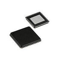
CYRF69213-40LFXC Cypress Semiconductor Corp, CYRF69213-40LFXC Datasheet - Page 39

CYRF69213-40LFXC
Manufacturer Part Number
CYRF69213-40LFXC
Description
IC PROC 8K FLASH 40VQFN
Manufacturer
Cypress Semiconductor Corp
Series
CYRFr
Type
Transceiverr
Datasheet
1.CYRF69213-40LFXC.pdf
(77 pages)
Specifications of CYRF69213-40LFXC
Package / Case
40-VQFN Exposed Pad, 40-HVQFN, 40-SQFN, 40-DHVQFN
Frequency
2.4GHz
Data Rate - Maximum
1Mbps
Modulation Or Protocol
ISM
Applications
General Purpose
Power - Output
4dBm
Sensitivity
-97dBm
Voltage - Supply
4 V ~ 5.5 V
Current - Receiving
23.4mA
Current - Transmitting
36.6mA
Data Interface
PCB, Surface Mount
Memory Size
8kB Flash, 256B SRAM
Antenna Connector
PCB, Surface Mount
Operating Temperature
0°C ~ 70°C
Operating Frequency
2497 MHz
Operating Supply Voltage
2.5 V or 3.3 V
Maximum Operating Temperature
+ 70 C
Minimum Operating Temperature
0 C
Mounting Style
SMD/SMT
Operating Temperature (min)
0C
Operating Temperature (max)
70C
Operating Temperature Classification
Commercial
Operating Supply Voltage (min)
1.8V
Operating Supply Voltage (typ)
2.5/3.3V
Operating Supply Voltage (max)
3.6V
Lead Free Status / RoHS Status
Lead free / RoHS Compliant
For Use With
770-1001 - ISP 4PORT CYPRESS ENCORE II MCU
Lead Free Status / Rohs Status
Lead free / RoHS Compliant
Other names
428-1934
Available stocks
Company
Part Number
Manufacturer
Quantity
Price
Part Number:
CYRF69213-40LFXC
Manufacturer:
CYPRESS/赛普拉斯
Quantity:
20 000
Table 50. P0.3/INT1–P0.4/INT2 Configuration (P03CR–P04CR) [0x08–0x09] [R/W]
Table 51. P0.7 Configuration (P07CR) [0x0C] [R/W]
Table 52. P1.0/D+ Configuration (P10CR) [0x0D] [R/W]
Document #: 001-07552 Rev. *D
Bit #
Field
Read/Write
Default
T
the INT0–INT2. These registers exist in all CYRF69213 parts. The INT0–INT2 interrupts are different than all the other GPIO
interrupts. These pins are connected directly to the interrupt controller to provide three edge-sensitive interrupts with independent
interrupt vectors. These interrupts occur on a rising edge when Int act Low is clear and on a falling edge when Int act Low is set.
These pins are enabled as interrupt sources in the interrupt controller registers
To use these pins as interrupt inputs configure them as inputs by clearing the corresponding Output Enable. If the INT0–INT2
pins are configured as outputs with interrupts enabled, firmware can generate an interrupt by writing the appropriate value to the
P0.3 and P0.4 data bits in the P0 Data Register
Regardless of whether the pins are used as Interrupt or GPIO pins the Int Enable, Int act Low, TTL Threshold, Open Drain, and
Pull up Enable bits control the behavior of the pin
The P0.3/INT1–P0.4/INT2 pins are individually configured with the P03CR (0x08), and P04CR (0x09), respectively.
Note Changing the state of the Int Act Low bit can cause an unintentional interrupt to be generated. When configuring these
interrupt sources, it is best to follow the following procedure:
Bit #
Field
Read/Write
Default
This register controls the operation of pin P0.7.
Bit #
Field
Read/Write
Default
1. Disable interrupt source
2. Configure interrupt source
3. Clear any pending interrupts from the source
4. Enable interrupt source
hese registers control the operation of pins P0.3–P0.4, respectively. These pins are shared between the P0.3–P0.4 GPIOs and
Reserved
Reserved
R/W
7
–
0
7
–
0
7
0
Reserved
Int Enable
Int Enable
R/W
R/W
6
–
0
6
0
6
0
Int Act Low
Int Act Low
Int Act Low
R/W
R/W
R/W
5
0
5
0
5
0
TTL Thresh
TTL Thresh
R/W
R/W
4
0
4
0
4
–
0
Reserved
Reserved
Reserved
3
–
0
3
–
0
3
–
0
(Table 76
Open Drain
Open Drain
R/W
and
R/W
2
0
2
0
2
–
0
Table
74)
Pull up En-
Pull up En-
Reserved
able
R/W
able
R/W
1
0
1
0
1
–
0
CYRF69213
Output En-
Output En-
Output En-
Page 39 of 77
able
R/W
able
R/W
able
R/W
0
0
0
0
0
0
[+] Feedback


