MC13201FC Freescale Semiconductor, MC13201FC Datasheet
MC13201FC
Specifications of MC13201FC
Available stocks


Related parts for MC13201FC

MC13201FC Summary of contents
Page 1
... Freescale Semiconductor, Inc., 2005, 2006, 2007, 2008. All rights reserved. Document Number: MC13201 MC13201 Package Information Plastic Package Case 1311-03 Ordering Information Device MC13201FC MC13201FCR2 (Tape and Reel) Contents 1 Introduction . . . . . . . . . . . . . . . . . . . . . . . . . . 1 2 Features . . . . . . . . . . . . . . . . . . . . . . . . . . . . . 2 3 Block Diagrams . . . . . . . . . . . . . . . . . . . . . . . 4 4 Data Transfer Mode . . . . . . . . . . . . . . . . . . . . 5 ® 5 Electrical Characteristics . . . . . . . . . . . . . . . 7 6 Functional Description ...
Page 2
... Operates on one of 16 selectable channels in the 2.4 GHz band • dBm nominal output power, programmable from -27 dBm to +3 dBm typical • Receive sensitivity of <-91 dBm (typical PER, 20-byte packet, much better than the 802.15.4 Standard of -85 dBm 2 MC13201 Technical Data, Rev. 1.3, Freescale Semiconductor ...
Page 3
... Freescale provides a software suite to complement the MC13201 hardware which is called the Freescale Simple MAC (SMAC): • Simple proprietary wireless connectivity. • Small memory footprint (about 3 Kbytes typical) • Supports point-to-point and star network configurations • Proprietary networks • Source code and application examples provided Freescale Semiconductor MC13201 Technical Data, Rev. 1.3, 3 ...
Page 4
... P ow er-U p Digital C ontrol R egulator L Logic Digital P roc egulator tal R egulator eiv egulator A rbiter S equenc e M anager (C ontrol Logic ) bol A rbiter A rbiter G eneration Microcontroller ROM SPI (Flash) RAM CPU A/D Application Network MAC PHY Driver Freescale Semiconductor V DDA DDIN T V DDD V DDV ...
Page 5
... For both graphs, the required 802.15.4 Standard accuracy and range limits are shown. A 3.5 dBm offset has been programmed into the CCA reporting level to center the level over temperature in the graphs. Freescale Semiconductor 1 byte 125 bytes maximum FLI Payload Data Figure 3 ...
Page 6
... TX buffer. The MCU then requests that the MC13201 transmit the data. The MCU is notified via an interrupt when the whole packet has successfully been transmitted. 6 802.15.4 Accuracy and range Requirements -80 -70 Input Power (dBm) 802.15.4 Accuracy and Range Requirements -85 -75 -65 -55 -45 Input Power Level (dBm) MC13201 Technical Data, Rev. 1.3, -60 -50 -35 -25 -15 Freescale Semiconductor ...
Page 7
... Logic Input Voltage High SPI Clock Rate RF Input Power Crystal Reference Oscillator Frequency (±40 ppm over operating conditions to meet the 802.15.4 Standard the supply voltage is produced by a switching DC-DC converter, ripple should be less than 100 mV peak-to-peak. Freescale Semiconductor Table 1. Maximum Ratings Symbol V BATT, Vin P ...
Page 8
... CCH I CCD I CCI I CCT I CCR ) (All digital inputs MC13201 Technical Data, Rev. 1.3, Min Typ Max Unit - 0.2 2.5 µA - 1.0 22 µ 154 µA - 500 1500 µ ±1 µ 30 DDINT 70 DDINT V DDINT 80 DDINT V DDINT DDINT Section 8.3, “Low Freescale Semiconductor ...
Page 9
... Output Power Control Range Over the Air Data Rate 2nd Harmonic 3rd Harmonic 1 SPI Register 12 programmed to 0x00BC which sets output power to nominal (-1 dBm typical). 2 SPI Register 12 programmed to 0x00FF which sets output power to maximum. Freescale Semiconductor = 2 ° MHz, unless otherwise noted.) A ref Symbol SENS ...
Page 10
... SPI timing parameters are referenced to Min 125 50 50 250 6.8nH LDB212G4005C-001 3.9nH C2 10pF Figure 6. RF Parametric Evaluation Circuit 7. Current drain in the various modes is listed in MC13201 Technical Data, Rev. 1.3, Figure 8. Typ Max Not Mounted ANT1 1.0pF F_Antenna SMA_edge_Receptac 5 Table 3, DC Electrical Freescale Semiconductor Unit ...
Page 11
... CPHA = 0 and the clock polarity control bit CPOL = 0. 3. Master Out/Slave In (MOSI) - Incoming data from the host is presented on the MOSI input. 4. Master In/Slave Out (MISO) - The MC13201 presents data to the master on the MISO output. A typical interconnection to a microcontroller is shown in Freescale Semiconductor Definition NOTE Figure 7 ...
Page 12
... Valid SPI digital timing specifications are shown in 12 RxD MISO TxD MOSI Sclk SPICLK Chip Enable (CE) Figure 7. SPI Interface Figure 8. SPI Burst Valid T2 T3 Figure 8. SPI Single Burst Timing Diagram Table 6. MC13201 Technical Data, Rev. 1.3, MC13201 Shift Register Freescale Semiconductor ...
Page 13
... MC13201 Reference Manual, (MC13201RM) for more details on SPI registers and transaction types. An example SPI read transaction with a 2-byte payload is shown in CE Clock Burst SPICLK MISO MOSI Freescale Semiconductor Valid Valid Header Read data Figure 9. SPI Read Transaction Diagram MC13201 Technical Data, Rev. 1.3, Figure 9 ...
Page 14
... Not used when internal T/R switch is used. bias network when used with an external balun. Not used when internal T/R switch is used. Must be grounded for normal operation. See Footnote 1. See Footnote 1. See Footnote 1. See Footnote 1. Freescale Semiconductor ...
Page 15
... GPIO6 Digital Input/Output 1 25 GPIO7 Digital Input/Output 26 XTAL1 Input Freescale Semiconductor Description Active High. Low to high transition initiates sequence depending on SPI setting. Should be taken high after SPI programming to start sequence and should be held high through the sequence. After sequence is complete, return RXTXEN to low ...
Page 16
... VDDLO2 externally and to PAO± through a bias network. Note: Do not use this pin to supply circuitry external to the chip. External paddle / flag ground. MC13201 Technical Data, Rev. 1.3, Functionality Connect to 16 MHz crystal and load capacitor. Decouple to ground. Decouple to ground. Decouple to ground. Connect to ground. Freescale Semiconductor ...
Page 17
... RFIN_M 2 RFIN_P 3 CT_Bias PAO_P 6 PAO_M GPIO4 9 Freescale Semiconductor MC13201 Figure 10. Pin Connections (Top View) MC13201 Technical Data, Rev. 1. GPIO6 23 GPIO5 22 VDDINT 21 VDDD 20 IRQ MISO 17 MOSI 16 17 ...
Page 18
... The on-chip trim capability may be used to determine the closest standard value by adjusting the trim value via the SPI and observing the frequency at CLKO. Each internal trim load capacitor has a trim range of approximately steps. Initial tolerance for the internal trim capacitance is approximately ±15%. 18 MC13201 Technical Data, Rev. 1.3, Freescale Semiconductor ...
Page 19
... Equivalent series resistance 6 Load capacitance Shunt capacitance Mode of oscillation 1 User must be sure manufacturer specifications apply to the desired package wider frequency tolerance may acceptable if application uses trimming at production final test. Freescale Semiconductor U6 26 XTAL1 Y 1 16MHz 27 XTAL2 MC1320x Y1 = Daishinku KDS - DSX321G ZD00882 Figure 11 ...
Page 20
... Use only STOP2 and STOP3 modes (not STOP1) with these devices where the GPIO states are retained. The MCU must retain control of the MC13201 IO during low power operation. — As stated above all unused GPIO should be programmed as outputs low for lowest power and no floating inputs. 20 NOTE MC13201 Technical Data, Rev. 1.3, Freescale Semiconductor ...
Page 21
... RFIN_x and PAO_x signal pairs. The RF interface allows both single port differential operation and dual port differential operation. RFIN_P (PAO_P RFIN_M (PAO_M) 3 CT_Bias 5 PAO_P 6 PAO_M Freescale Semiconductor RX LNA SW ITCH RX ENABLE PA2 PA2 ENABLE CT_Bias Generator CT_Bias CONTROL PA1 FROM TX PSM PA1 ENABLE Figure 12 ...
Page 22
... Separate RFIN and PAO signals are provided for connection with the baluns, and the CT_bias signal is programmed to provide the external switch control. The polarity of the external switch control is selectable. 22 RFIN_P (PAO_P) Balun RFIN_M (PAO_M) CT_Bia s MC13201 Bypass PAO_P PAO_M MC13201 Technical Data, Rev. 1.3, Freescale Semiconductor ...
Page 23
... L5 provide DC-biasing to VDDA but are ac-isolated. CT_Bias is not required or used. VDD LNA Ant Sw Balun Bypass Balun Bypass Using External Antenna Switch with LNA Figure 14. Dual Port RF Configuration Examples Freescale Semiconductor RFIN_P (PAO_P) RFIN_M (PAO_M) MC13201 CT_Bia s PAO_P VDDA PAO_M RX Antenna L2 ...
Page 24
... Register 07 with the RF interface control bits Register r/w r/w r/w r 0x0C00 Figure 15. Control_B Register 07 Model Operation. The use of CT_Bias pin in Dual Port Mode is controlled MC13201 Technical Data, Rev. 1.3, 0x07 r/w r Section 8.5.1, “Single Port Freescale Semiconductor ...
Page 25
... Freescale Semiconductor Table 10. RF Interface Control Bits 1 = CT_Bias enabled. Output state is defined CT_Bias disabled. Output state is tri-stated. The output state of CT_Bias under varying conditions is defined in has effect for dual port operation CT_Bias inverted CT_Bias not inverted 1= Single Port Mode selected where RF switch is active and RFIN_M and RFIN_P and bidirectional signals ...
Page 26
... PAO_M 5 1.8nH PAO_P 2 RFIN_P 1 RFIN_M 3 CT_Bias L4 MC1320x 1.8nH Figure 16. RF Single Port Application with an F-Antenna 26 RF_switch_mode CT_Bias_inv 6.8nH LDB212G4005C-001 3.9nH C2 10pF MC13201 Technical Data, Rev. 1.3, CT_Bias (Low-Z) X Hi-Z X Unknown Not Mounted ANT1 1.0pF F_Antenna SMA_edge_Receptac 5 Freescale Semiconductor ...
Page 27
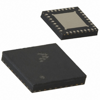
... 0.5 32X 0.3 VIEW M-M ( (1.73) 0.065 32X 0.015 (0.25) DETAIL N PREFERRED CORNER CONFIGURATION 4 DETAIL T DETAIL M BACKSIDE PIN 1 INDEX OPTION Figure 17. Outline Dimensions for QFN-32, 5x5 mm Freescale Semiconductor 0 NOTES: B DETAIL M PIN 1 INDEX 32 1 0.25 0.5 28X 0.30 32X 0.18 M 0.1 ...
Page 28
... Freescale Semiconductor products are not designed, intended, or authorized for use as components in systems intended for surgical implant into the body, or other applications intended to support or sustain life, or for any other application in which the failure of the Freescale Semiconductor product could create a situation where personal injury or death may occur. Should Buyer purchase ...