DEMOKITCRX14 STMicroelectronics, DEMOKITCRX14 Datasheet - Page 28
DEMOKITCRX14
Manufacturer Part Number
DEMOKITCRX14
Description
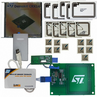
RFID EVALUATION KIT ISO14443-B
Manufacturer
STMicroelectronics
Type
Development kitr
Specifications of DEMOKITCRX14
Contents
CD-ROM, CRX14 Board, USB Transceiver, Samples and Documentation
Processor To Be Evaluated
CRX14
Interface Type
I2C
Operating Supply Voltage
5 V
For Use With/related Products
CRX14
Lead Free Status / RoHS Status
Contains lead / RoHS non-compliant
Other names
497-3704
Available stocks
Company
Part Number
Manufacturer
Quantity
Price
Company:

Part Number:
DEMOKITCRX14
Manufacturer:
HITACHI
Quantity:
340


CRX14 ISO14443 type-B radio frequency data transfer
6.5
Figure 23. Wave received using BPSK sub-carrier modulation
6.6
28/47
1/847kHz
V RFIN
Input RF data transfer from the PICC to the CRX14 (answer
frame)
The CRX14 uses the ISO14443 type-B retro-modulation scheme which is demodulated and
decoded by the RF
The modulation is obtained by modifying the PICC current consumption (load modulation).
This load modulation induces an H-field variation, by coupling, that is detected by the
CRX14 RF
variation and decodes the information received from the PICC.
Data must be transmitted using a 847kHz, BPSK modulated sub-carrier frequency, f
shown in
(from ‘0’ to ‘1’ or from ‘1’ to ‘0’) are encoded by phase shift keying the sub-carrier.
Transmission format of answer frame characters
The PICC should use the same character format as that used for output data transfer (see
Figure
An Answer Frame includes the SOF, data, CRC and the EOF, as illustrated in
data transfer rate is 106 kbit/s.
The CRX14 will also accept Answer Frames that do not contain the SOF and EOF
delimiters, provided that these Frames are correctly set in the Parameter Register. (See
Figure
20).
26).
Figure
IN
input as a voltage variation on the antenna. The RF
23, and as specified in ISO14443 type-B. In BPSK, all data state transitions
IN
circuitry.
phase shift
1/106kHz
Doc ID 8880 Rev 4
V OFFSET
V
RET
V DYN
IN
PICC data bit to be transmitted
to the CRX14.
847kHz BPSK, resulting signal
generated by the PICC for the
load modulation.
input demodulates this
t
Load modulation effect on
the H-Field received on the
CRX14 RF IN input pad
Figure
26. The
S
CRX14
ai09253
, as
Related parts for DEMOKITCRX14
Image
Part Number
Description
Manufacturer
Datasheet
Request
R

Part Number:
Description:
DEMO KIT M24LR-64-R
Manufacturer:
STMicroelectronics
Datasheet:

Part Number:
Description:
STMicroelectronics [RIPPLE-CARRY BINARY COUNTER/DIVIDERS]
Manufacturer:
STMicroelectronics
Datasheet:
Part Number:
Description:
STMicroelectronics [LIQUID-CRYSTAL DISPLAY DRIVERS]
Manufacturer:
STMicroelectronics
Datasheet:

Part Number:
Description:
BOARD EVAL FOR MEMS SENSORS
Manufacturer:
STMicroelectronics
Datasheet:
Part Number:
Description:
NPN TRANSISTOR POWER MODULE
Manufacturer:
STMicroelectronics
Datasheet:
Part Number:
Description:
TURBOSWITCH ULTRA-FAST HIGH VOLTAGE DIODE
Manufacturer:
STMicroelectronics
Datasheet:
Part Number:
Description:
Manufacturer:
STMicroelectronics
Datasheet:
Part Number:
Description:
DIODE / SCR MODULE
Manufacturer:
STMicroelectronics
Datasheet:
Part Number:
Description:
DIODE / SCR MODULE
Manufacturer:
STMicroelectronics
Datasheet:
Part Number:
Description:
Search -----> STE16N100
Manufacturer:
STMicroelectronics
Datasheet:
Part Number:
Description:
Search ---> STE53NA50
Manufacturer:
STMicroelectronics
Datasheet:
Part Number:
Description:
NPN Transistor Power Module
Manufacturer:
STMicroelectronics
Datasheet: