APT65GP60JDQ2 Microsemi Power Products Group, APT65GP60JDQ2 Datasheet - Page 2
APT65GP60JDQ2
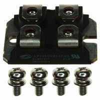
Manufacturer Part Number
APT65GP60JDQ2
Description
IGBT 600V 130A 431W SOT227
Manufacturer
Microsemi Power Products Group
Series
POWER MOS 7®r
Datasheet
1.APT65GP60JDQ2.pdf
(9 pages)
Specifications of APT65GP60JDQ2
Igbt Type
PT
Configuration
Single
Voltage - Collector Emitter Breakdown (max)
600V
Vce(on) (max) @ Vge, Ic
2.7V @ 15V, 65A
Current - Collector (ic) (max)
130A
Current - Collector Cutoff (max)
1.25mA
Input Capacitance (cies) @ Vce
7.4nF @ 25V
Power - Max
431W
Input
Standard
Ntc Thermistor
No
Mounting Type
Chassis Mount
Package / Case
ISOTOP
Lead Free Status / RoHS Status
Lead free / RoHS Compliant
Other names
APT65GP60JDQ2MI
APT65GP60JDQ2MI
APT65GP60JDQ2MI


THERMAL AND MECHANICAL CHARACTERISTICS
1 Repetitive Rating: Pulse width limited by maximum junction temperature.
2 For Combi devices, I
3 See MIL-STD-750 Method 3471.
4 E
5 E
6 E
Symbol
Symbol
V
SSOA
adding to the IGBT turn-on loss. (See Figure 24.)
loss. (See Figures 21, 22.)
APT Reserves the right to change, without notice, the specifications and information contained herein.
V
Isolation
t
t
t
t
R
R
C
E
E
E
E
C
C
Q
Q
d(on)
d(off)
E
d(on)
d(off)
E
W
on1
on2
off
Q
GEP
on1
on2
on1
on2
θ
θ
oes
t
t
t
t
res
ies
ge
off
off
gc
r
r
f
f
JC
JC
g
T
is the clamped inductive turn-off energy measured in accordance with JEDEC standard JESD24-1. (See Figures 21, 23.)
is the clam ped inductive turn-on-energy of the IGBT only, without the effect of a commutating diode reverse recovery current
is the clamped inductive turn-on energy that includes a commutating diode reverse recovery current in the IGBT turn-on switching
Characteristic
Input Capacitance
Output Capacitance
Reverse Transfer Capacitance
Gate-to-Emitter Plateau Voltage
Total Gate Charge
Gate-Emitter Charge
Gate-Collector ("Miller ") Charge
Switching Safe Operating Area
Turn-on Delay Time
Current Rise Time
Turn-off Delay Time
Current Fall Time
Turn-on Switching Energy
Turn-on Switching Energy (Diode)
Turn-off Switching Energy
Turn-on Delay Time
Current Rise Time
Turn-off Delay Time
Current Fall Time
Turn-on Switching Energy
Turn-on Switching Energy (Diode)
Turn-off Switching Energy
Characteristic
Junction to Case (IGBT)
Junction to Case (DIODE)
Package Weight
RMS Voltage
ces
includes both IGBT and FRED leakages
(50-60hHz Sinusoidal Wavefomr Ffrom Terminals to Mounting Base for 1 Min.)
3
6
6
4
4
4
55
5
Inductive Switching (125°C)
15V, L = 100µH,V
Inductive Switching (25°C)
T
J
= 150°C, R
V
GE
Test Conditions
Capacitance
Gate Charge
= 0V, V
T
V
V
V
T
V
V
V
f = 1 MHz
J
CC
CC
CE
I
I
I
R
J
R
GE
GE
GE
C
C
C
= +125°C
= +25°C
G
G
= 65A
= 65A
= 65A
= 300V
= 400V
= 400V
= 5Ω
= 5Ω
= 15V
= 15V
= 15V
G
CE
= 5Ω, V
CE
= 25V
= 600V
GE
=
2500
MIN
250
MIN
7400
1410
1925
1470
TYP
580
210
605
895
130
605
29.2
TYP
7.5
35
50
65
30
55
90
65
30
55
90
MAX
MAX
1.21
.29
UNIT
UNIT
°C/W
Volts
nC
pF
µ
µ
gm
ns
ns
V
A
J
J
Related parts for APT65GP60JDQ2
Image
Part Number
Description
Manufacturer
Datasheet
Request
R

Part Number:
Description:
IGBT 600V 100A 463W TO247
Manufacturer:
Microsemi Power Products Group
Datasheet:

Part Number:
Description:
IGBT 600V 198A 833W TO264
Manufacturer:
Microsemi Power Products Group
Datasheet:
Part Number:
Description:
IGBT 600V 41A 187W TO247
Manufacturer:
Microsemi Power Products Group
Datasheet:
Part Number:
Description:
MOSFET N-CH 600V 23A TO-247
Manufacturer:
Microsemi Power Products Group
Datasheet:

Part Number:
Description:
MOSFET N-CH 500V 17A TO-220
Manufacturer:
Microsemi Power Products Group
Datasheet:
Part Number:
Description:
MOSFET N-CH 1200V 3.5A TO-220
Manufacturer:
Microsemi Power Products Group
Datasheet:
Part Number:
Description:
MOSFET N-CH 500V 22A TO-247
Manufacturer:
Microsemi Power Products Group
Datasheet:
Part Number:
Description:
MOSFET N-CH 100V 75A TO-247
Manufacturer:
Microsemi Power Products Group
Datasheet:
Part Number:
Description:
MOSFET N-CH 200V 56A TO-247
Manufacturer:
Microsemi Power Products Group
Datasheet:
Part Number:
Description:
MOSFET N-CH 500V 27A TO-247
Manufacturer:
Microsemi Power Products Group
Datasheet:
Part Number:
Description:
MOSFET N-CH 300V 40A TO-247
Manufacturer:
Microsemi Power Products Group
Datasheet:
Part Number:
Description:
MOSFET N-CH 200V 59A TO-247
Manufacturer:
Microsemi Power Products Group
Datasheet:
Part Number:
Description:
MOSFET N-CH 500V 26A TO-247
Manufacturer:
Microsemi Power Products Group
Datasheet:
Part Number:
Description:
MOSFET N-CH 300V 40A TO-247
Manufacturer:
Microsemi Power Products Group
Datasheet:
Part Number:
Description:
MOSFET N-CH 200V 65A TO-247
Manufacturer:
Microsemi Power Products Group
Datasheet: