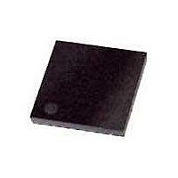
XR18W750IL48-F Exar Corporation, XR18W750IL48-F Datasheet - Page 3

XR18W750IL48-F
Manufacturer Part Number
XR18W750IL48-F
Description
IC WIRELESS UART CTRLR 48QFN
Manufacturer
Exar Corporation
Datasheet
1.XR18W750IL48-F.pdf
(44 pages)
Specifications of XR18W750IL48-F
Package / Case
48-VFQFN Exposed Pad
Function
Controller
Rf Type
General Purpose
Secondary Attributes
I²C Interface
Processor Series
XR18W750
Core
8051
Data Bus Width
8 bit
Data Ram Size
32 KB
Interface Type
I2C, UART
Maximum Clock Frequency
400 KHz
Number Of Timers
1
Operating Supply Voltage
2.25 V to 3.63 V
Maximum Operating Temperature
+ 85 C
Mounting Style
SMD/SMT
3rd Party Development Tools
PK51, CA51, A51, ULINK2
Development Tools By Supplier
XR18W750/753-0A-EB, XR18W750/753-0B-EB
Minimum Operating Temperature
- 40 C
Program Memory Type
EEPROM
Lead Free Status / RoHS Status
Lead free / RoHS Compliant
Lead Free Status / RoHS Status
Lead free / RoHS Compliant, Lead free / RoHS Compliant
Available stocks
Company
Part Number
Manufacturer
Quantity
Price
Company:
Part Number:
XR18W750IL48-F
Manufacturer:
EXAR
Quantity:
120
Part Number:
XR18W750IL48-F
Manufacturer:
EXAR/艾科嘉
Quantity:
20 000
Pin Description
REV. 1.0.0
PIN DESCRIPTIONS
PARALLEL MODE INTERFACE SIGNALS
SERIAL MODE INTERFACE SIGNALS
TXRDY#
RXRDY#
(R/W#)
(IRQ#)
(VCC)
IOW#
N
IOR#
CS#
INT
RX
A2
A1
A0
D7
D6
D5
D4
D3
D2
D1
D0
TX
AME
48-QFN
P
23
22
21
34
33
32
31
30
29
28
27
26
18
19
47
35
20
44
43
IN
#
T
I/O
YPE
O
O
O
O
I
I
I
I
I
Address data lines [2:0]. These 3 address lines select one of the internal regis-
ters in the UART during a data bus transaction. The internal UART registers are
not accessed by the 8051 microprocessor in the parallel mode.
Data bus lines [7:0] (bidirectional).
When 16/68# pin is HIGH, the Intel bus interface is selected and this input
becomes read strobe (active low). The falling edge instigates an internal read
cycle and retrieves the data byte from an internal register pointed by the address
lines [A2:A0], puts the data byte on the data bus to allow the host processor to
read it on the rising edge.
When 16/68# pin is LOW, the Motorola bus interface is selected and this input is
not used and should be connected to VCC.
When 16/68# pin is HIGH, it selects Intel bus interface and this input becomes
write strobe (active low). The falling edge instigates the internal write cycle and
the rising edge transfers the data byte on the data bus to an internal register
pointed by the address lines.
When 16/68# pin is LOW, the Motorola bus interface is selected and this input
becomes read (HIGH) and write (LOW) signal.
Chip select (active low) signal.
When 16/68# pin is HIGH for Intel bus interface, this output is an active high
interrupt output. Upon power-up, this output is in three-state mode. The output
state is controlled by the user through the software setting of MCR[3]. The INT
output is enabled when MCR[3] is set to a logic 1. See MCR[3].
When 16/68# pin is LOW for Motorola bus interface, this output becomes an
active low, open drain interrupt output. An external pull-up resistor is required for
proper operation.
UART Transmitter Ready (active low). The output provides the TX FIFO/THR sta-
tus for transmit. See
UART Receiver Ready (active low). This output provides the RX FIFO/RHR sta-
tus for receive. See
UART Transmit Data. Standard transmit and receive interface is enabled when
MCR[6] = 0. In this mode, the TX signal will be HIGH during reset or idle (no
data). If this pin is not used, leave it unconnected.
UART Receive Data. Normal receive data input must idle HIGH. If this pin is not
used, tie it to VCC or pull it high via a 100k ohm resistor.
3
Table 3
Table 3
. If it is not used, leave it unconnected.
. If it is not used, leave it unconnected.
D
ESCRIPTION
WIRELESS UART CONTROLLER
XR18W750


