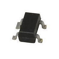
BF1108,215 NXP Semiconductors, BF1108,215 Datasheet

BF1108,215
Specifications of BF1108,215
Available stocks
Related parts for BF1108,215
BF1108,215 Summary of contents
Page 1
BF1108; BF1108R Silicon RF switches Rev. 04 — 29 May 2008 1. Product profile 1.1 General description These switches are a combination of a depletion type Field-Effect Transistor (FET) and a band-switching diode in an SOT143B (BF1108) or SOT143R (BF1108R) ...
Page 2
... NXP Semiconductors 2. Pinning information Table 2. Pin BF1108 (SOT143B BF1108R (SOT143R [1] Drain and source are interchangeable. 3. Ordering information Table 3. Type number BF1108 BF1108R 4. Marking Table 4. Type number BF1108 BF1108R BF1108_BF1108R_4 Product data sheet Pinning Description FET gate; diode anode diode cathode source drain FET gate ...
Page 3
... NXP Semiconductors 5. Limiting values Table 5. In accordance with the Absolute Maximum Rating System (IEC 60134). Symbol FET Diode FET and diode T stg Thermal characteristics Table 6. Symbol R th(j-sp) [1] Soldering point of FET gate and diode anode lead. 7. Static characteristics Table unless otherwise specified. ...
Page 4
... NXP Semiconductors 8. Dynamic characteristics Table 8. Common cathode; T Symbol Parameter FET and diode L ins(on) ISL off R DSon Diode [ diode forward current the series connection [3] Guaranteed on AQL basis; inspection level S4, AQL 1.0. BF1108_BF1108R_4 Product data sheet Dynamic characteristics = 25 C. amb Conditions on-state insertion loss ...
Page 5
... NXP Semiconductors 0 L ins(on 400 forward current). Measured in test circuit see Fig 1. On-state insertion loss as a function of frequency; typical values On-state Off-state Fig 3. Test circuit BF1108_BF1108R_4 Product data sheet mgs357 ISL off 800 1200 f (MHz (diode F Figure 3. Fig 2. Off-state isolation as a function of frequency; ...
Page 6
... NXP Semiconductors 9. Package outline Plastic surface-mounted package; 4 leads DIMENSIONS (mm are the original dimensions UNIT max 1.1 0.48 0.88 0.1 mm 0.9 0.38 0.78 OUTLINE VERSION IEC SOT143B Fig 4. Package outline SOT143B BF1108_BF1108R_4 Product data sheet scale 0.15 3.0 1.4 1.9 1.7 0.09 2 ...
Page 7
... NXP Semiconductors Plastic surface-mounted package; reverse pinning; 4 leads DIMENSIONS (mm are the original dimensions UNIT max 1.1 0.48 0.88 0.1 mm 0.9 0.38 0.78 OUTLINE VERSION IEC SOT143R Fig 5. Package outline SOT143R BF1108_BF1108R_4 Product data sheet scale 0.15 3.0 1.4 1.9 1.7 0.09 2 ...
Page 8
... Data sheet status Product data sheet • The format of this data sheet has been redesigned to comply with the new identity guidelines of NXP Semiconductors. • Legal texts have been adapted to the new company name where appropriate. • Symbol notation has been adapted to comply with the current guidelines of NXP Semiconductors ...
Page 9
... Right to make changes — NXP Semiconductors reserves the right to make changes to information published in this document, including without limitation specifications and product descriptions, at any time and without notice ...
Page 10
... NXP Semiconductors 14. Contents 1 Product profi 1.1 General description 1.2 Features . . . . . . . . . . . . . . . . . . . . . . . . . . . . . . 1 1.3 Applications . . . . . . . . . . . . . . . . . . . . . . . . . . . 1 1.4 Quick reference data Pinning information . . . . . . . . . . . . . . . . . . . . . . 2 3 Ordering information . . . . . . . . . . . . . . . . . . . . . 2 4 Marking . . . . . . . . . . . . . . . . . . . . . . . . . . . . . . . . 2 5 Limiting values Thermal characteristics Static characteristics Dynamic characteristics . . . . . . . . . . . . . . . . . . 4 9 Package outline . . . . . . . . . . . . . . . . . . . . . . . . . 6 10 Abbreviations . . . . . . . . . . . . . . . . . . . . . . . . . . . 8 11 Revision history . . . . . . . . . . . . . . . . . . . . . . . . . 8 12 Legal information ...


