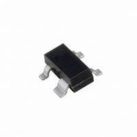
BF998,235 NXP Semiconductors, BF998,235 Datasheet

BF998,235
Specifications of BF998,235
Related parts for BF998,235
BF998,235 Summary of contents
Page 1
DATA SHEET BF998; BF998R Silicon N-channel dual-gate MOS-FETs Product specification Supersedes data of April 1991 DISCRETE SEMICONDUCTORS 1996 Aug 01 ...
Page 2
... NXP Semiconductors Silicon N-channel dual-gate MOS-FETs FEATURES Short channel transistor with high forward transfer admittance to input capacitance ratio Low noise gain controlled amplifier GHz. APPLICATIONS VHF and UHF applications with 12 V supply voltage, such as television tuners and professional communications equipment ...
Page 3
... NXP Semiconductors Silicon N-channel dual-gate MOS-FETs LIMITING VALUES In accordance with the Absolute Maximum Rating System (IEC 134). SYMBOL PARAMETER V drain-source voltage DS I drain current D I gate 1 current G1 I gate 2 current G2 P total power dissipation; BF998 tot P total power dissipation; BF998R tot ...
Page 4
... NXP Semiconductors Silicon N-channel dual-gate MOS-FETs THERMAL CHARACTERISTICS SYMBOL R thermal resistance from junction to ambient in free air; BF998 th j-a R thermal resistance from junction to ambient in free air; BF998R note 1 th j-a Notes 1. Device mounted on a ceramic substrate 0.7 mm. 2. Device mounted on a printed-circuit board. ...
Page 5
... NXP Semiconductors Silicon N-channel dual-gate MOS-FETs 24 handbook, halfpage I D (mA G2-S amb Fig.5 Output characteristics; typical values. 24 handbook, halfpage I D (mA −1600 −1200 −800 = 25 G2-S amb Fig.7 Drain current as a function of gate 1 voltage; typical values. 1996 Aug 01 MGE813 handbook, halfpage V G1-S = ...
Page 6
... NXP Semiconductors Silicon N-channel dual-gate MOS-FETs 30 handbook, halfpage | (mS − amb Fig.9 Forward transfer admittance as a function of gate 1 voltage; typical values. 2.3 handbook, halfpage C is (pF) 2.1 1.9 1.7 1.5 1.3 −2.4 −1.6 −0 MHz G2-S amb Fig.11 Gate 1 input capacitance as a function of gate 1-source voltage ...
Page 7
... NXP Semiconductors Silicon N-channel dual-gate MOS-FETs (mS mA G2-S D amb Fig.13 Input admittance as a function of the frequency; typical values (mS) ϕ mA G2-S D amb Fig.15 Forward transfer admittance and phase as a function of frequency; typical values. 1996 Aug 01 MGC466 (MHz C. MGC468 2 10 ϕ fs (deg) ...
Page 8
... NXP Semiconductors Silicon N-channel dual-gate MOS-FETs handbook, full pagewidth C1 5 Ω input 140 kΩ mS 0.5 mS nH; 4 turns 0.8 mm copper wire, internal diameter 4 mm 160 nH; 3 turns 0.8 mm copper wire, internal diameter 8 mm. Tapped at approximately half a turn from the cold side, to adjust G ...
Page 9
... NXP Semiconductors Silicon N-channel dual-gate MOS-FETs V DD handbook, full pagewidth 100 kΩ Ω input 3 200 nH; 11 turns 0.5 mm copper wire, without spacing, internal diameter 3 mm cm, silvered 0.8 mm copper wire above ground plane cm, silvered 0.5 mm copper wire above ground plane. ...
Page 10
... NXP Semiconductors Silicon N-channel dual-gate MOS-FETs 0 handbook, halfpage ΔG tr (dB) −10 −20 −30 I DSS = −40 max typ min − 200 MHz amb Fig.19 Automatic gain control characteristics measured in circuit of Fig.17. 1996 Aug 01 MGE808 handbook, halfpage agc ( BF998; BF998R 0 ΔG tr (dB) I DSS = − ...
Page 11
... NXP Semiconductors Silicon N-channel dual-gate MOS-FETs PACKAGE OUTLINES Plastic surface-mounted package; 4 leads DIMENSIONS (mm are the original dimensions UNIT max 1.1 0.48 0.88 0.1 mm 0.9 0.38 0.78 OUTLINE VERSION IEC SOT143B 1996 Aug scale 0.15 3.0 1.4 1.9 1.7 0.09 2.8 1.2 ...
Page 12
... NXP Semiconductors Silicon N-channel dual-gate MOS-FETs Plastic surface-mounted package; reverse pinning; 4 leads DIMENSIONS (mm are the original dimensions UNIT max 1.1 0.48 0.88 0.1 mm 0.9 0.38 0.78 OUTLINE VERSION IEC SOT143R 1996 Aug scale 0.15 3.0 1.4 1.9 1.7 0.09 2.8 1.2 ...
Page 13
... In no event shall NXP Semiconductors be liable for any indirect, incidental, punitive, special or consequential damages (including - without limitation - lost profits, lost savings, business interruption, costs related to the ...
Page 14
... NXP Semiconductors’ specifications such use shall be solely at customer’s own risk, and (c) customer fully indemnifies NXP Semiconductors for any liability, damages or failed product claims resulting from customer design and use of the product for automotive applications beyond NXP Semiconductors’ ...
Page 15
... Interface, Security and Digital Processing expertise Customer notification This data sheet was changed to reflect the new company name NXP Semiconductors, including new legal definitions and disclaimers. No changes were made to the technical content, except for package outline drawings which were updated to the latest version. ...


