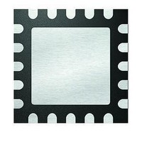
MCP4461T-103E/ML Microchip Technology, MCP4461T-103E/ML Datasheet - Page 53

MCP4461T-103E/ML
Manufacturer Part Number
MCP4461T-103E/ML
Description
IC DGTL POT 257TAPS 10K 20QFN
Manufacturer
Microchip Technology
Datasheet
1.MCP4441-103EML.pdf
(100 pages)
Specifications of MCP4461T-103E/ML
Package / Case
20-VFQFN Exposed Pad
Temperature Coefficient
150 ppm/°C Typical
Taps
257
Resistance (ohms)
10K
Number Of Circuits
4
Memory Type
Non-Volatile
Interface
I²C, 2-Wire Serial
Voltage - Supply
2.7 V ~ 5.5 V
Operating Temperature
-40°C ~ 125°C
Mounting Type
Surface Mount
Number Of Pots
Quad
Taps Per Pot
257
Resistance
10 KOhms
Wiper Memory
Non Volatile
Buffered Wiper
Buffered
Digital Interface
I2C
Operating Supply Voltage
2.7 V to 5.5 V
Supply Current
600 uA
Maximum Operating Temperature
+ 125 C
Minimum Operating Temperature
- 40 C
Description/function
Quad I2C Digital POT with Nonvolatile Memory
Mounting Style
SMD/SMT
Supply Voltage (max)
5.5 V
Supply Voltage (min)
2.7 V
Lead Free Status / RoHS Status
Lead free / RoHS Compliant
Available stocks
Company
Part Number
Manufacturer
Quantity
Price
Part Number:
MCP4461T-103E/ML
Manufacturer:
MICROCHIP/微芯
Quantity:
20 000
6.0
The MCP44XX devices support the I
The MCP44XX I
(does not generate the serial clock).
Figure 6-1
I
The MCP44XX devices use the two-wire I
interface. This interface can operate in standard, fast or
High-Speed mode. A device that sends data onto the
bus is defined as transmitter, and a device receiving
data as receiver. The bus has to be controlled by a
master device which generates the serial clock (SCL),
controls the bus access and generates the START and
STOP conditions. The MCP44XX device works as
slave. Both master and slave can operate as
transmitter or receiver, but the master device
determines which mode is activated. Communication is
initiated by the master (microcontroller) which sends
the START bit, followed by the slave address byte. The
first byte transmitted is always the slave address byte,
which contains the device code, the address bits, and
the R/W bit.
Refer to the Phillips I
the I
FIGURE 6-1:
Diagram.
© 2010 Microchip Technology Inc.
2
C interface signals are high-voltage tolerant.
Typical I
Controller
Note 1: If High voltage commands are desired,
2
Host
C specifications.
I/O
SCL
SDA
2: These pins have internal pull-ups. If
3: This pin could be tied high, low, or
SERIAL INTERFACE (I
shows a typical I
2
(1)
C Interface Connections
some type of external circuitry needs to
be implemented.
faster rise times are required, then
external pull-ups should be added.
connected to an I/O pin of the Host
Controller.
2
C’s module operates in Slave mode
2
C document for more details of
Typical I
2
C Interface connection. All
2
C Interface Block
2
C serial protocol.
SCL
HVC/A0
A1
SDA
2
MCP4XXX
C)
(2, 3)
2
C serial
(2)
6.1
The I
are:
• SDA (Serial Data)
• SCL (Serial Clock)
• A0 (Address 0 bit)
• A1 (Address 1 bit)
6.1.1
The Serial Data (SDA) signal is the data signal of the
device. The value on this pin is latched on the rising
edge of the SCL signal when the signal is an input.
With the exception of the START and STOP conditions,
the high or low state of the SDA pin can only change
when the clock signal on the SCL pin is low. During the
high period of the clock, the SDA pin’s value (high or
low) must be stable. Changes in the SDA pin’s value
while the SCL pin is HIGH will be interpreted as a
START or a STOP condition.
6.1.2
The Serial Clock (SCL) signal is the clock signal of the
device. The rising edge of the SCL signal latches the
value on the SDA pin. The MCP44XX supports three
I
• Standard Mode: clock rates up to 100 kHz
• Fast Mode: clock rates up to 400 kHz
• High-Speed Mode (HS mode): clock rates up to
The MCP44XX will not stretch the clock signal (SCL)
since memory read access occur fast enough.
Depending on the clock rate mode, the interface will
display different characteristics.
6.1.3
There are up to two hardware pins used to specify the
device address. The number of address pins is
determined by the part number.
Address 0 is multiplexed with the High Voltage
Command (HVC) function. So the state of A0 is latched
on the MCP4XXX’s POR/BOR event.
The state of the A1 pin should be static, that is they
should be tied high or tied low.
6.1.3.1
The High Voltage Command (HVC) signal is
multiplexed with Address 0 (A0) and is used to indicate
that the command, or sequence of commands, are in
the High Voltage mode. High Voltage commands allow
the device’s WiperLock Technology and write protect
features to be enabled and disabled.
The HVC pin has an internal resistor connection to the
MCP44XXs internal V
2
C interface clock modes:
3.4 MHz
2
C interface uses up to four pins (signals). These
Signal Descriptions
SERIAL DATA (SDA)
SERIAL CLOCK (SCL)
THE ADDRESS BITS (A1:A0)
The High Voltage Command (HVC)
Signal
MCP444X/446X
DD
signal.
DS22265A-page 53


