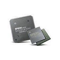
S1D13743F00A200 Epson, S1D13743F00A200 Datasheet - Page 132

S1D13743F00A200
Manufacturer Part Number
S1D13743F00A200
Description
LCD Drivers LCD CNTRL w/Embedded 464KB SRAM
Manufacturer
Epson
Datasheet
1.S1D13743F00A200.pdf
(134 pages)
Specifications of S1D13743F00A200
Maximum Clock Frequency
33 MHz, 68.59 MHz
Operating Supply Voltage
1.5 V
Maximum Operating Temperature
+ 85 C
Package / Case
QFP-20-144
Attached Touch Screen
No
Maximum Supply Current
74 mA
Minimum Operating Temperature
- 40 C
Lead Free Status / RoHS Status
Lead free / RoHS Compliant
Available stocks
Company
Part Number
Manufacturer
Quantity
Price
Company:
Part Number:
S1D13743F00A200
Manufacturer:
EPSON
Quantity:
5 690
- Current page: 132 of 134
- Download datasheet (3Mb)
Page 132
S1D13743
X70A-A-001-02
• section 7.3.1, added information about PWRSVE pin to TFT Power-On sequence note 1
• section 7.3.1, in second note changed LCD pins VD[35:0] to VD[23:0]
• section 7.3.2, added information about PWRSVE pin to TFT Power-Off sequence note 1
• section 7.3.2, in second note changed LCD pins VD[35:0] to VD[23:0]
• section 7.3.3, added 18-bit panel data (VD[17:0])
• section 7.3.3, fixed REG reference for PCLK Polarity, should be “REG[28h] bit 7”
• section 8.1, removed arrow pointing down from the Clock Source Select
• section 9.2, added register set summary table
• REG[04h] bits 5-0, updated the M-Divide Ratio table to read “REG[04h] bits 5-0”
• REG[06h] ~ REG[0Ch], changed the bit descriptions for the PLL Setting Registers 0-3,
• REG[14h] bit 7, combined the note under the VD Data Swap bit into the main bit
• REG[2Ah] - remove text “bit 7-4 Reserved”
• REG[2Ch] bit 6, updated the YRC Reset bit description
• REG[34h] bit 7, updated the Display Blank bit description
• REG[48h] ~ REG[49h], changed the default value for the Memory Data Port Registers
• REG[54h], changed the default value for the Gamma Correction Table Data Register to
• REG[58h] bit 4, updated the YYC Last Line bit description and removed reference to
• REG[5Ah] ~ REG[64h], minor wording clarifications to the GPIO registers
• section 10, changed “Horizontal Period” to “Horizontal Display Width” and “Vertical
• section 10, added cross reference to Display Interface timing section for Panel Timing
• section 11, updated the Intel 80, 8-bit Interface Color Formats diagrams to use the
• section 12, updated the Intel 80, 16-bit Interface Color Formats diagrams to use the
• section 13, updated the YUV Timing diagrams to use the proper 13743 pin names
• section 14, added data input to LUT
instead of “REG[2Ah] bit 7”
instead of “bits 6-0” and changed the maximum value from 7Fh to 3Fh
reserved all individual bit descriptions and added specific programming values for each
register
description and added references to the exact tables
to “not applicable”
“not applicable”
the MESSI interface (should be Intel 80 interface)
Period” to “Vertical Display Height”
Parameter definitions
proper 13743 pin names
proper 13743 pin names
Revision 2.7
Epson Research and Development
Hardware Functional Specification
Vancouver Design Center
Issue Date: 2010/05/18
Related parts for S1D13743F00A200
Image
Part Number
Description
Manufacturer
Datasheet
Request
R

Part Number:
Description:
Display Modules & Development Tools S1D13743 Eval board
Manufacturer:
Epson

Part Number:
Description:
INK CARTRIDGE, T0803, EPSON, MAG
Manufacturer:
Epson
Datasheet:

Part Number:
Description:
INK CARTRIDGE, T0804, EPSON, YEL
Manufacturer:
Epson
Datasheet:

Part Number:
Description:
CXA1034M
Manufacturer:
EPSON Electronics
Datasheet:

Part Number:
Description:
Manufacturer:
EPSON Electronics
Datasheet:

Part Number:
Description:
Manufacturer:
EPSON Electronics
Datasheet:

Part Number:
Description:
Manufacturer:
EPSON Electronics
Datasheet:

Part Number:
Description:
Manufacturer:
EPSON Electronics
Datasheet:

Part Number:
Description:
RTC58321Real time clock module(4-bit I/O CONNECTION REAL TIME CLOCK MODULE)
Manufacturer:
EPSON Electronics
Datasheet:

Part Number:
Description:
SCI7661DC-DC Converter
Manufacturer:
EPSON Electronics
Datasheet:

Part Number:
Description:
Manufacturer:
EPSON Electronics
Datasheet:

Part Number:
Description:
Manufacturer:
EPSON Electronics
Datasheet:


