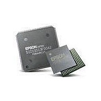
S1D13743F00A200 Epson, S1D13743F00A200 Datasheet - Page 15

S1D13743F00A200
Manufacturer Part Number
S1D13743F00A200
Description
LCD Drivers LCD CNTRL w/Embedded 464KB SRAM
Manufacturer
Epson
Datasheet
1.S1D13743F00A200.pdf
(134 pages)
Specifications of S1D13743F00A200
Maximum Clock Frequency
33 MHz, 68.59 MHz
Operating Supply Voltage
1.5 V
Maximum Operating Temperature
+ 85 C
Package / Case
QFP-20-144
Attached Touch Screen
No
Maximum Supply Current
74 mA
Minimum Operating Temperature
- 40 C
Lead Free Status / RoHS Status
Lead free / RoHS Compliant
Available stocks
Company
Part Number
Manufacturer
Quantity
Price
Company:
Part Number:
S1D13743F00A200
Manufacturer:
EPSON
Quantity:
5 690
- Current page: 15 of 134
- Download datasheet (3Mb)
4.2.2 LCD Interface
4.2.3 Clocks
CLKOUTEN
Pin Name
Pin Name
CLKOUT
VD[23:0]
Epson Research and Development
Vancouver Design Center
PCLK
Hardware Functional Specification
Issue Date: 2010/05/18
CLKI
VS
HS
DE
Type
Type
IO
O
O
O
O
O
I
I
K10, L3, L4,
K4, K5, K6,
K7, K8, K9,
L5, L6, L7,
J4, J5, J6,
J7, J8, J9,
H10, H11,
J10, J11,
FCBGA
FCBGA
L8, L9
Pin #
Pin #
D10
D11
C11
D9
A4
A3
B4
Note
Note
The LCD interface requires a separate power rail (PIOVDD) to support the configurable
IO drive. For details, see the CNF2 description in Section 4.3, “Summary of Configura-
tion Options” on page 18.
The input function of VD[23:0] is used for production test only.
12,13,60,
55,50,45,
40,20,14,
15,61,56,
51,48,44,
38,21,63,
62,57,54,
49,43,39
Pin #
Pin #
QFP
QFP
115
110
112
5
4
8
3
Table 4-2: LCD Interface Pin Descriptions
Table 4-3: Clock Input Pin Descriptions
DSEL
Cell
HB_
Cell
HIS
HO
HO
HO
HO
HO
HI
PIOVDD
PIOVDD
PIOVDD
PIOVDD
PIOVDD
Voltage
Voltage
IOVDD
IOVDD
IOVDD
IO
IO
Revision 2.7
RESET#
RESET#
State
Input
Input
State
CLKI
L
H
H
L
L
Power
Status
Power
Status
Save
Input
CLKI
Input
Save
L
L
L
L
L
MHz input for PLL operation or MHz input if PLL
is bypassed.
This output pin represents the CLKI pin if
enabled by CLKOUTEN. When disabled, the
output is low.
Note: This output is not affected by the various
power save modes.
This pin enables/disables the CLKOUT pin.
Panel Data lines pins 23-0.
Note: The Panel Data Lines can be swapped
(i.e. VD23 = VD0) using the VD Data Swap bit,
REG[14h] bit 7.
Note: The VD output drive is selectable
between 2.5mA and 6.5mA using the CNF2
pin. For details, see Section 4.3, “Summary of
Configuration Options” on page 18.
This output pin is the Vertical Sync pulse.
This output pin is the Horizontal Sync pulse.
This output pin is the Data Clock.
This output pin is the Data Enable.
Description
Description
X70A-A-001-02
S1D13743
Page 15
Related parts for S1D13743F00A200
Image
Part Number
Description
Manufacturer
Datasheet
Request
R

Part Number:
Description:
Display Modules & Development Tools S1D13743 Eval board
Manufacturer:
Epson

Part Number:
Description:
INK CARTRIDGE, T0803, EPSON, MAG
Manufacturer:
Epson
Datasheet:

Part Number:
Description:
INK CARTRIDGE, T0804, EPSON, YEL
Manufacturer:
Epson
Datasheet:

Part Number:
Description:
CXA1034M
Manufacturer:
EPSON Electronics
Datasheet:

Part Number:
Description:
Manufacturer:
EPSON Electronics
Datasheet:

Part Number:
Description:
Manufacturer:
EPSON Electronics
Datasheet:

Part Number:
Description:
Manufacturer:
EPSON Electronics
Datasheet:

Part Number:
Description:
Manufacturer:
EPSON Electronics
Datasheet:

Part Number:
Description:
RTC58321Real time clock module(4-bit I/O CONNECTION REAL TIME CLOCK MODULE)
Manufacturer:
EPSON Electronics
Datasheet:

Part Number:
Description:
SCI7661DC-DC Converter
Manufacturer:
EPSON Electronics
Datasheet:

Part Number:
Description:
Manufacturer:
EPSON Electronics
Datasheet:

Part Number:
Description:
Manufacturer:
EPSON Electronics
Datasheet:


