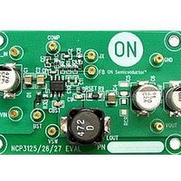
NCP3125AGEVB ON Semiconductor, NCP3125AGEVB Datasheet

NCP3125AGEVB
Specifications of NCP3125AGEVB
Related parts for NCP3125AGEVB
NCP3125AGEVB Summary of contents
Page 1
NCP3125 4 A Synchronous PWM Switching Converter The NCP3125 is a flexible synchronous PWM Switching Buck Regulator. The NCP3125 is capable of producing output voltages as low as 0.8 V. The NCP3125 also incorporates voltage mode control. To reduce the ...
Page 2
VREF + 0.8 V − FB COMP Clock Ramp OSC OSC AGND Table 1. PIN DESCRIPTION Pin Pin Name 1 PGND The PGND pin is the high current ground pin for the low−side MOSFET and the ...
Page 3
Table 2. MAXIMUM RATINGS Rating Main Supply Voltage Input Bootstrap Supply Voltage vs GND Bootstrap Supply Voltage vs Ground (spikes ≤ 50 ns) Bootstrap Pin Voltage High Side Switch Max DC Current V Pin Voltage SW Switching ...
Page 4
Table 3. ELECTRICAL CHARACTERISTICS min/max values unless otherwise noted.) Characteristic Input Voltage Range Boost Voltage Range SUPPLY CURRENT Quiescent Supply Current Shutdown Supply Current Boost Quiescent Current UNDER VOLTAGE LOCKOUT V UVLO Threshold IN V UVLO Hysteresis IN SWITCHING REGULATOR ...
Page 5
3.5 3 2.5 2.0 −60 −40 − JUNCTION TEMPERATURE (°C) J Figure 4. I vs. Temperature ...
Page 6
Figure 10. Duty Cycle Maximum vs. Temperature 100 5.0 V Output 1 0.5 1 ...
Page 7
General The NCP3125 is a PWM synchronous buck regulator intended to supply load for DC−DC conversion from 5 V and 12 V buses. The NCP3125 is a regulator that has integrated high−side and low−side NMOSFETs ...
Page 8
V COMP BG TG Figure 17. Enable/Disable Driver State Diagram External Soft−Start The NCP3125 features an external soft−start function, which reduces inrush current and overshoot of the output voltage. Soft−start is achieved by using the internal current source of ...
Page 9
... ON Semiconductor has a Microsoft Excel® based design tool available online under the design tools section of the NCP3125 product page. The tool allows you to capture your design point and optimize the performance of your regulator based on your design criteria ...
Page 10
ESR of electrolytic capacitors. The ratio of ripple current to maximum output current is given in Equation Iout ...
Page 11
DCR ³ _DC RMS 2 281 mW + 4. Inductor RMS current RMS DCR = Inductor DC resistance LP = Inductor DC power dissipation CU_DC The core losses and AC ...
Page 12
In a typical converter design, the ESR of the output capacitor bank dominates the transient response. Please note that DV and DV are out of phase with each OUT−DIS OUT−ESR other, and the larger of these two voltages will determine ...
Page 13
When calculating the rise time and fall time of the high side MOSFET it is important to know the charge characteristic shown in Figure 22. Vth Figure 22. MOSFET Switching Characteristics RISE I ...
Page 14
The formula for calculating the junction temperature with the package in free air is Power dissipation of the Thermal resistance junction to ...
Page 15
... The values can be adjusted in real time using the compensation tool comp calc, available for download at ON Semiconductor’s website. The value of the feed through resistor should always be at least 2X the value of R noise. Using the 2X assumption, R ...
Page 16
0. 31 Feed through capacitor ...
Page 17
cross LC C 1.355 3.102 kHz Compensation capacitance Output capacitor ESR ESR C = Output capacitance OUT f = ...
Page 18
Assuming an output capacitance of 470 mF in parallel with 22 mF with a crossover frequency of 35 kHz, the compensation values for common output voltages can be calculated as shown in Table 6: Table 6. COMPENSATION VALUES V V ...
Page 19
ICinrush_RMS CIN ESR e 5 CIN ESR 0.316 t DELAY_TOTAL 380 0.1 W 16.45 ms 0.1W 330 0.1 W 330 mF 0.316 16.45 ...
Page 20
Output Voltage Output Current tss Figure 28. Resistive Load Current Alternatively, if the output has an under voltage lockout, turns defined voltage level, and draws a consistent current, then the RMS connected load current is ...
Page 21
VIN C1 C3 10uF 470uF 4 16V 16V Vin RC 806R GND_IN COMP CP CC 1.8nF 120n 50V 10V Figure 31. Standard Application 1 VIN 10uF 3 10uF ...
Page 22
... *For additional information on our Pb−Free strategy and soldering details, please download the ON Semiconductor Soldering and Mounting Techniques Reference Manual, SOLDERRM/D. ON Semiconductor and are registered trademarks of Semiconductor Components Industries, LLC (SCILLC). SCILLC reserves the right to make changes without further notice to any products herein. SCILLC makes no warranty, representation or guarantee regarding the suitability of its products for any particular purpose, nor does SCILLC assume any liability arising out of the application or use of any product or circuit, and specifically disclaims any and all liability, including without limitation special, consequential or incidental damages. “ ...


