NCP3125AGEVB ON Semiconductor, NCP3125AGEVB Datasheet - Page 20
NCP3125AGEVB
Manufacturer Part Number
NCP3125AGEVB
Description
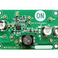
Power Management Modules & Development Tools NCP3125 Evaluation Board
Manufacturer
ON Semiconductor
Type
DC/DC Switching Converters, Regulators & Controllersr
Datasheets
1.NCP3125AGEVB.pdf
(22 pages)
2.NCP3125AGEVB.pdf
(1 pages)
3.NCP3125AGEVB.pdf
(4 pages)
4.NCP3125AGEVB.pdf
(1 pages)
Specifications of NCP3125AGEVB
Maximum Operating Temperature
+ 125 C
Minimum Operating Temperature
- 40 C
Operating Supply Voltage
4.5 V to 13.2 V
Product
Power Management Modules
For Use With/related Products
NCP3125
Lead Free Status / RoHS Status
Lead free / RoHS Compliant


turns on at a defined voltage level, and draws a consistent
current, then the RMS connected load current is:
I
V
V
If the inrush current is higher than the steady state input
current during max load, then an input fuse should be rated
accordingly using I
OUT
OUT
OUT_TO
Alternatively, if the output has an under voltage lockout,
I
CLI+
798 mA +
Figure 29. Voltage Enable Load Current
Voltage
Current
Output
Output
Figure 28. Resistive Load Current
V
OUT
* V
= Output current
= Output voltage
= Output voltage load turn on
V
2
OUT
t methodology.
1.0 V
OUT_TO
3.3 V * 1.2 V
3.3 V
tss
tss
Voltage
Current
Output
Output
I
OUT
t
3.3 V
1 A
3.3 V
(eq. 51)
http://onsemi.com
20
Layout Considerations
very important. Switching current from one power device to
another can generate voltage transients across the
impedances of the interconnecting bond wires and circuit
traces. The interconnecting impedances should be
minimized by using wide short printed circuit traces. The
critical components should be located as close together as
possible using ground plane construction or single point
grounding. For optimal performance, the NCP3125 should
have a layout similar to the one shown in Figure 30. An
important note is that the input voltage to the NCP3125
should have local decoupling to PGND. The recommended
decoupling for input voltage is a 1 mF general purpose
ceramic capacitor and a 0.01 mF COG ceramic capacitor
placed in parallel.
for output electrolytic and ceramic bulk capacitors,
respectively.
PGND
Single Point
PGND
As in any high frequency switching regulator, layout is
The typical applications are shown in Figures 31 and 32
Grounding
Î Î
Î Î
AGND
ISET
VSW
BST
CF
VIN
Figure 30. Recommended Layout
CC
RC
Î Î
RF
R 2
R 1
CP
COMP
AGND
PGND
FB
Î Î Î Î Î
Î Î Î Î Î
Î Î Î Î Î
Î Î Î Î Î
Î Î Î Î Î
0.01 uF
1 .0 uF
COG
Bottom
Top
Î
Î
0.01 uF
1 .0 uF
COG
AGND
COMP
FB
PGND
AGND
CP
RF
R 1
R 2
CC
RC
BST
VIN
ISET
VSW
CF
Related parts for NCP3125AGEVB
Image
Part Number
Description
Manufacturer
Datasheet
Request
R

Part Number:
Description:
4 A Synchronous PWM Switching Converter
Manufacturer:
ON Semiconductor
Datasheet:
Part Number:
Description:
BOARD EVALUATION NCP3125 CERAMIC
Manufacturer:
ON Semiconductor
Datasheet:
Part Number:
Description:
ON Semiconductor [VOLTAGE REGULATOR]
Manufacturer:
ON Semiconductor
Datasheet:
Part Number:
Description:
357-036-542-201 CARDEDGE 36POS DL .156 BLK LOPRO
Manufacturer:
ON Semiconductor
Datasheet:
Part Number:
Description:
357-036-542-201 CARDEDGE 36POS DL .156 BLK LOPRO
Manufacturer:
ON Semiconductor
Datasheet:
Part Number:
Description:
357-036-542-201 CARDEDGE 36POS DL .156 BLK LOPRO
Manufacturer:
ON Semiconductor
Datasheet:
Part Number:
Description:
357-036-542-201 CARDEDGE 36POS DL .156 BLK LOPRO
Manufacturer:
ON Semiconductor
Datasheet:
Part Number:
Description:
357-036-542-201 CARDEDGE 36POS DL .156 BLK LOPRO
Manufacturer:
ON Semiconductor
Datasheet:
Part Number:
Description:
357-036-542-201 CARDEDGE 36POS DL .156 BLK LOPRO
Manufacturer:
ON Semiconductor
Datasheet:
Part Number:
Description:
357-036-542-201 CARDEDGE 36POS DL .156 BLK LOPRO
Manufacturer:
ON Semiconductor
Datasheet:
Part Number:
Description:
357-036-542-201 CARDEDGE 36POS DL .156 BLK LOPRO
Manufacturer:
ON Semiconductor
Datasheet:
Part Number:
Description:
357-036-542-201 CARDEDGE 36POS DL .156 BLK LOPRO
Manufacturer:
ON Semiconductor
Datasheet:
Part Number:
Description:
357-036-542-201 CARDEDGE 36POS DL .156 BLK LOPRO
Manufacturer:
ON Semiconductor
Datasheet:
Part Number:
Description:
Manufacturer:
ON Semiconductor
Datasheet: