NCP3125AGEVB ON Semiconductor, NCP3125AGEVB Datasheet - Page 9
NCP3125AGEVB
Manufacturer Part Number
NCP3125AGEVB
Description
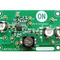
Power Management Modules & Development Tools NCP3125 Evaluation Board
Manufacturer
ON Semiconductor
Type
DC/DC Switching Converters, Regulators & Controllersr
Datasheets
1.NCP3125AGEVB.pdf
(22 pages)
2.NCP3125AGEVB.pdf
(1 pages)
3.NCP3125AGEVB.pdf
(4 pages)
4.NCP3125AGEVB.pdf
(1 pages)
Specifications of NCP3125AGEVB
Maximum Operating Temperature
+ 125 C
Minimum Operating Temperature
- 40 C
Operating Supply Voltage
4.5 V to 13.2 V
Product
Power Management Modules
For Use With/related Products
NCP3125
Lead Free Status / RoHS Status
Lead free / RoHS Compliant


Current Limit Protection
conduct large currents. The regulator will latch off,
protecting the load and MOSFETs from excessive heat and
damage. Low−side R
of each LS−FET turn−on duration to sense the current.
While the low side MOSFET is on, the V
compared to the user set internally generated OCP trip
voltage. If the V
an overcurrent condition occurs and a counter counts
consecutive current trips. If the counter reaches 7, the PWM
logic and both HS−FET and LS−FET are turned off. The
regulator has to go through a Power On Reset (POR) cycle
to reset the OCP fault as shown in Figure 20.
Design Procedure
important to collect as much information as possible about
the behavior of the input and output before starting the
design.
tool available online under the design tools section of the
NCP3125 product page. The tool allows you to capture your
design point and optimize the performance of your regulator
based on your design criteria.
are LC filtered to produce a lower DC output voltage V
The output voltage can be changed by modifying the on time
relative to the switching period T or switching frequency.
The ratio of high side switch on time to the switching period
is called duty ratio D. Duty ratio can also be calculated using
Table 4. DESIGN PARAMETERS
Input voltage
Output voltage
Input ripple voltage
Output ripple voltage
Output current rating
Operating frequency
In case of an overload, the low−side (LS) FET will
When starting the design of a buck regulator, it is
ON Semiconductor has a Microsoft Excel® based design
The buck converter produces input voltage V
Design Parameter
SW
voltage is lower than OCP trip voltage,
DS(on)
(V
(V
(V
(V
(I
(F
OUT
SW
IN
OUT
INRIPPLE
OUTRIPPLE
sense is implemented at the end
)
)
)
)
)
)
10.8 V to 13.2 V
Example Value
SW
350 kHz
300 mV
60 mV
IN
3.3 V
4 A
APPLICATION SECTION
pulses that
voltage is
http://onsemi.com
OUT
.
9
MOSFET
V
the High Side Switch Voltage Drop V
D
F
T
T
T
V
V
V
V
Inductor Selection
rule of thumb for the design where the percentage of ripple
current in the inductor should be between 10% and 40%.
When using ceramic output capacitors, the ripple current can
be greater because the ESR of the output capacitor is smaller,
thus a user might select a higher ripple current. However,
Low Side
F
D +
D +
SW
OFF
ON
PHASE
VOCTH
SW
OUT
HSD
IN
LSD
OUT
Current
When selecting an inductor, the designer can employ a
Drive
+ 1
T
V
, V
BG
0 V
T
ON
IN
T
V
IN
* V
OUT
and (1 * D) +
, the Low Side Switch Voltage Drop V
−
HSD
+
Figure 20. Current Limit Trip
) V
) V
= Duty cycle
= Switching frequency
= Switching period
= High side switch off time
= High side switch on time
= High side switch voltage drop
= Input voltage
= Low side switch voltage drop
= Output voltage
LSD
VOCTH
LSD
T
[ D +
OFF
T
BG
V
V
OUT
IN
HSD
³ 27.5% +
.
LSD
Current
Flow
(eq. 2)
(eq. 3)
(eq. 4)
3.3 V
12 V
, and
Related parts for NCP3125AGEVB
Image
Part Number
Description
Manufacturer
Datasheet
Request
R

Part Number:
Description:
4 A Synchronous PWM Switching Converter
Manufacturer:
ON Semiconductor
Datasheet:
Part Number:
Description:
BOARD EVALUATION NCP3125 CERAMIC
Manufacturer:
ON Semiconductor
Datasheet:
Part Number:
Description:
ON Semiconductor [VOLTAGE REGULATOR]
Manufacturer:
ON Semiconductor
Datasheet:
Part Number:
Description:
357-036-542-201 CARDEDGE 36POS DL .156 BLK LOPRO
Manufacturer:
ON Semiconductor
Datasheet:
Part Number:
Description:
357-036-542-201 CARDEDGE 36POS DL .156 BLK LOPRO
Manufacturer:
ON Semiconductor
Datasheet:
Part Number:
Description:
357-036-542-201 CARDEDGE 36POS DL .156 BLK LOPRO
Manufacturer:
ON Semiconductor
Datasheet:
Part Number:
Description:
357-036-542-201 CARDEDGE 36POS DL .156 BLK LOPRO
Manufacturer:
ON Semiconductor
Datasheet:
Part Number:
Description:
357-036-542-201 CARDEDGE 36POS DL .156 BLK LOPRO
Manufacturer:
ON Semiconductor
Datasheet:
Part Number:
Description:
357-036-542-201 CARDEDGE 36POS DL .156 BLK LOPRO
Manufacturer:
ON Semiconductor
Datasheet:
Part Number:
Description:
357-036-542-201 CARDEDGE 36POS DL .156 BLK LOPRO
Manufacturer:
ON Semiconductor
Datasheet:
Part Number:
Description:
357-036-542-201 CARDEDGE 36POS DL .156 BLK LOPRO
Manufacturer:
ON Semiconductor
Datasheet:
Part Number:
Description:
357-036-542-201 CARDEDGE 36POS DL .156 BLK LOPRO
Manufacturer:
ON Semiconductor
Datasheet:
Part Number:
Description:
357-036-542-201 CARDEDGE 36POS DL .156 BLK LOPRO
Manufacturer:
ON Semiconductor
Datasheet:
Part Number:
Description:
Manufacturer:
ON Semiconductor
Datasheet: