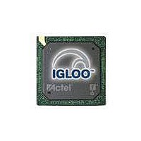
AGL250V5-FGG144 Actel, AGL250V5-FGG144 Datasheet - Page 13

AGL250V5-FGG144
Manufacturer Part Number
AGL250V5-FGG144
Description
FPGA - Field Programmable Gate Array 250K System Gates
Manufacturer
Actel
Datasheet
1.AGL030V2-CSG81.pdf
(236 pages)
Specifications of AGL250V5-FGG144
Processor Series
AGL250
Core
IP Core
Maximum Operating Frequency
892.86 MHz
Number Of Programmable I/os
97
Data Ram Size
36864
Supply Voltage (max)
1.575 V
Maximum Operating Temperature
+ 70 C
Minimum Operating Temperature
0 C
Development Tools By Supplier
AGL-Icicle-Kit, AGL-Dev-Kit-SCS, Silicon-Explorer II, Silicon-Sculptor 3, SI-EX-TCA, FlashPro 4, FlashPro 3, FlashPro Lite
Mounting Style
SMD/SMT
Supply Voltage (min)
1.425 V
Number Of Gates
250 K
Package / Case
FPBGA-144
Lead Free Status / RoHS Status
Lead free / RoHS Compliant
Available stocks
Company
Part Number
Manufacturer
Quantity
Price
Company:
Part Number:
AGL250V5-FGG144
Manufacturer:
Microsemi SoC
Quantity:
10 000
- Current page: 13 of 236
- Download datasheet (8Mb)
All six CCC blocks are usable; the four corner CCCs and the east CCC allow simple clock delay
operations as well as clock spine access.
The inputs of the six CCC blocks are accessible from the FPGA core or from one of several inputs
located near the CCC that have dedicated connections to the CCC block.
The CCC block has these key features:
Additional CCC specifications:
Global Clocking
IGLOO devices have extensive support for multiple clocking domains. In addition to the CCC and PLL
support described above, there is a comprehensive global clock distribution network.
Each VersaTile input and output port has access to nine VersaNets: six chip (main) and three quadrant
global networks. The VersaNets can be driven by the CCC or directly accessed from the core via
multiplexers (MUXes). The VersaNets can be used to distribute low-skew clock signals or for rapid
distribution of high-fanout nets.
I/Os with Advanced I/O Standards
The IGLOO family of FPGAs features a flexible I/O structure, supporting a range of voltages (1.2 V, 1.5 V,
1.8 V, 2.5 V, 3.0 V wide range, and 3.3 V). IGLOO FPGAs support many different I/O standards—single-
ended and differential.
The I/Os are organized into banks, with two or four banks per device. The configuration of these banks
determines the I/O standards supported
Table 1 • I/O Standards Supported
I/O Bank Type
Advanced
Standard Plus North and south banks of AGL250 and
Standard
•
•
•
•
•
•
•
•
•
•
Wide input frequency range (f
Output frequency range (f
2 programmable delay types for clock skew minimization
Clock frequency synthesis (for PLL only)
Internal phase shift = 0°, 90°, 180°, and 270°. Output phase shift depends on the output divider
configuration (for PLL only).
Output duty cycle = 50% ± 1.5% or better (for PLL only)
Low output jitter: worst case < 2.5% × clock period peak-to-peak period jitter when single global
network used (for PLL only)
Maximum acquisition time is 300 µs (for PLL only)
Exceptional tolerance to input period jitter—allowable input jitter is up to 1.5 ns (for PLL only)
Four precise phases; maximum misalignment between adjacent phases of 40 ps × 250 MHz /
f
OUT_CCC
East and west banks of AGL250 and
larger devices
larger devices
All banks of AGL060 and AGL125K
All banks of AGL015 and AGL030
(for PLL only)
Device and Bank Location
OUT_CCC
IN_CCC
(Table
) = 0.75 MHz up to 250 MHz
) = 1.5 MHz up to 250 MHz
R ev i si o n 1 8
1).
LVCMOS
LVTTL/
✓
✓
✓
I/O Standards Supported
IGLOO Low Power Flash FPGAs
PCI/PCI-X
supported
Not
✓
✓
B-LVDS, M-LVDS
LVPECL, LVDS,
Not supported
Not supported
✓
1 -7
Related parts for AGL250V5-FGG144
Image
Part Number
Description
Manufacturer
Datasheet
Request
R

Part Number:
Description:
PQFP 100/FPGA, 6144 CLBS, 250000 GATES, 108 MHz
Manufacturer:
Actel

Part Number:
Description:
FPGA - Field Programmable Gate Array 250K System Gates
Manufacturer:
Actel
Datasheet:

Part Number:
Description:
FPGA - Field Programmable Gate Array 250K System Gates
Manufacturer:
Actel
Datasheet:

Part Number:
Description:
FPGA - Field Programmable Gate Array 250K System Gates
Manufacturer:
Actel
Datasheet:

Part Number:
Description:
FPGA - Field Programmable Gate Array 250K System Gates
Manufacturer:
Actel
Datasheet:

Part Number:
Description:
MCU, MPU & DSP Development Tools Silicon Sculptor Programming Mod
Manufacturer:
Actel

Part Number:
Description:
MCU, MPU & DSP Development Tools InSystem Programming ProASICPLUS Devices
Manufacturer:
Actel

Part Number:
Description:
Programming Socket Adapters & Emulators PQ160 Module
Manufacturer:
Actel

Part Number:
Description:
Programming Socket Adapters & Emulators Axcelerator Adap Module Kit
Manufacturer:
Actel

Part Number:
Description:
Programming Socket Adapters & Emulators Evaluation
Manufacturer:
Actel


