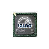
AGL250V5-FGG144 Actel, AGL250V5-FGG144 Datasheet - Page 19

AGL250V5-FGG144
Manufacturer Part Number
AGL250V5-FGG144
Description
FPGA - Field Programmable Gate Array 250K System Gates
Manufacturer
Actel
Datasheet
1.AGL030V2-CSG81.pdf
(236 pages)
Specifications of AGL250V5-FGG144
Processor Series
AGL250
Core
IP Core
Maximum Operating Frequency
892.86 MHz
Number Of Programmable I/os
97
Data Ram Size
36864
Supply Voltage (max)
1.575 V
Maximum Operating Temperature
+ 70 C
Minimum Operating Temperature
0 C
Development Tools By Supplier
AGL-Icicle-Kit, AGL-Dev-Kit-SCS, Silicon-Explorer II, Silicon-Sculptor 3, SI-EX-TCA, FlashPro 4, FlashPro 3, FlashPro Lite
Mounting Style
SMD/SMT
Supply Voltage (min)
1.425 V
Number Of Gates
250 K
Package / Case
FPBGA-144
Lead Free Status / RoHS Status
Lead free / RoHS Compliant
Available stocks
Company
Part Number
Manufacturer
Quantity
Price
Company:
Part Number:
AGL250V5-FGG144
Manufacturer:
Microsemi SoC
Quantity:
10 000
- Current page: 19 of 236
- Download datasheet (8Mb)
Figure 2-2 • V2 Devices – I/O State as a Function of VCCI and VCC Voltage Levels
Deactivation trip point:
Activation trip point:
V
V
a
d
= 0.85 V ± 0.2 V
= 0.75 V ± 0.2 V
VCC = 1.575 V
VCC = 1.14 V
Thermal Characteristics
Introduction
The temperature variable in the Actel Designer software refers to the junction temperature, not the
ambient temperature. This is an important distinction because dynamic and static power consumption
cause the chip junction to be higher than the ambient temperature.
EQ 1
where:
T
ΔT = Temperature gradient between junction (silicon) and ambient ΔT = θ
θ
P = Power dissipation
A
ja
= Ambient Temperature
= Junction-to-ambient of the package. θ
V
T
CC
J
can be used to calculate junction temperature.
= Junction Temperature = ΔT + T
Region 1: I/O Buffers are OFF
VCC = VCCI + VT
where VT can be from 0.58 V to 0.9 V (typically 0.75 V)
Deactivation trip point:
Activation trip point:
V
V
a
d
= 0.9 V ± 0.15 V
= 0.8 V ± 0.15 V
Region 1: I/O buffers are OFF
Region 2: I/O buffers are ON.
I/Os are functional (except differential inputs)
but slower because VCCI/VCC are below
specification. For the same reason, input
buffers do not meet VIH/VIL levels, and
output buffers do not meet VOH/VOL levels.
buffers do not meet VOH / VOL levels.
meet VIH / VIL levels, and output
same reason, input buffers do not
below specification. For the
but slower because VCCI is
A
(except differential
(except differential inputs)
ja
I/Os are functional
I/Os are functional
R ev i si o n 1 8
numbers are located in
buffers are ON.
buffers are ON.
Region 4: I/O
Region 4: I/O
standard; i.e., 1.14 V,1.425 V, 1.7 V,
Min VCCI datasheet specification
voltage at a selected I/O
2.3 V, or 3.0 V
Region 3: I/O buffers are ON.
I/Os are functional; I/O DC
specifications are met,
but I/Os are slower because
the VCC is below specification.
speed, VIH / VIL , VOH / VOL , etc.
Region 5: I/O buffers are ON
and power supplies are within
specification.
I/Os meet the entire datasheet
and timer specifications for
Table 2-5 on page
ja
* P
IGLOO Low Power Flash FPGAs
2-6.
VCCI
EQ 1
2 -5
Related parts for AGL250V5-FGG144
Image
Part Number
Description
Manufacturer
Datasheet
Request
R

Part Number:
Description:
PQFP 100/FPGA, 6144 CLBS, 250000 GATES, 108 MHz
Manufacturer:
Actel

Part Number:
Description:
FPGA - Field Programmable Gate Array 250K System Gates
Manufacturer:
Actel
Datasheet:

Part Number:
Description:
FPGA - Field Programmable Gate Array 250K System Gates
Manufacturer:
Actel
Datasheet:

Part Number:
Description:
FPGA - Field Programmable Gate Array 250K System Gates
Manufacturer:
Actel
Datasheet:

Part Number:
Description:
FPGA - Field Programmable Gate Array 250K System Gates
Manufacturer:
Actel
Datasheet:

Part Number:
Description:
MCU, MPU & DSP Development Tools Silicon Sculptor Programming Mod
Manufacturer:
Actel

Part Number:
Description:
MCU, MPU & DSP Development Tools InSystem Programming ProASICPLUS Devices
Manufacturer:
Actel

Part Number:
Description:
Programming Socket Adapters & Emulators PQ160 Module
Manufacturer:
Actel

Part Number:
Description:
Programming Socket Adapters & Emulators Axcelerator Adap Module Kit
Manufacturer:
Actel

Part Number:
Description:
Programming Socket Adapters & Emulators Evaluation
Manufacturer:
Actel


