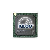
AGL250V5-FGG144 Actel, AGL250V5-FGG144 Datasheet - Page 32

AGL250V5-FGG144
Manufacturer Part Number
AGL250V5-FGG144
Description
FPGA - Field Programmable Gate Array 250K System Gates
Manufacturer
Actel
Datasheet
1.AGL030V2-CSG81.pdf
(236 pages)
Specifications of AGL250V5-FGG144
Processor Series
AGL250
Core
IP Core
Maximum Operating Frequency
892.86 MHz
Number Of Programmable I/os
97
Data Ram Size
36864
Supply Voltage (max)
1.575 V
Maximum Operating Temperature
+ 70 C
Minimum Operating Temperature
0 C
Development Tools By Supplier
AGL-Icicle-Kit, AGL-Dev-Kit-SCS, Silicon-Explorer II, Silicon-Sculptor 3, SI-EX-TCA, FlashPro 4, FlashPro 3, FlashPro Lite
Mounting Style
SMD/SMT
Supply Voltage (min)
1.425 V
Number Of Gates
250 K
Package / Case
FPBGA-144
Lead Free Status / RoHS Status
Lead free / RoHS Compliant
Available stocks
Company
Part Number
Manufacturer
Quantity
Price
Company:
Part Number:
AGL250V5-FGG144
Manufacturer:
Microsemi SoC
Quantity:
10 000
- Current page: 32 of 236
- Download datasheet (8Mb)
IGLOO DC and Switching Characteristics
2- 18
1. If a PLL is used to generate more than one output clock, include each output clock in the formula by adding its corresponding
contribution (P
Combinatorial Cells Contribution—P
Routing Net Contribution—P
I/O Input Buffer Contribution—P
I/O Output Buffer Contribution—P
RAM Contribution—P
PLL Contribution—P
P
P
P
P
P
P
C-CELL
NET
INPUTS
OUTPUTS
MEMORY
PLL
AC13
N
α
page
F
N
N
α
page
F
N
α
F
N
α
β
F
N
F
β
F
β
page
= P
F
= (N
* F
CLK
CLK
CLK
CLK
READ-CLOCK
WRITE-CLOCK
CLKOUT
1
2
3
C-CELL
S-CELL
C-CELL
INPUTS
OUTPUTS
BLOCKS
1
1
2
2
= N
= N
is the I/O buffer enable rate—guidelines are provided in
is the RAM enable rate for read operations.
DC4
is the RAM enable rate for write operations—guidelines are provided in
is the I/O buffer toggle rate—guidelines are provided in
is the I/O buffer toggle rate—guidelines are provided in
CLKOUT
is the toggle rate of VersaTile outputs—guidelines are provided in
is the toggle rate of VersaTile outputs—guidelines are provided in
S-CELL
= P
= N
is the global clock signal frequency.
is the global clock signal frequency.
is the global clock signal frequency.
is the global clock signal frequency.
2-19.
2-19.
2-19.
C-CELL
INPUTS
+ P
AC11
OUTPUTS
is the number of VersaTiles used as combinatorial modules in the design.
is the number of VersaTiles used as sequential modules in the design.
is the number of VersaTiles used as combinatorial modules in the design.
is the number of I/O input buffers used in the design.
is the output clock frequency.
is the number of RAM blocks used in the design.
product) to the total PLL contribution.
AC13
is the number of I/O output buffers used in the design.
+ N
*
* N
*
α
is the memory read clock frequency.
C-CELL
is the memory write clock frequency.
α
PLL
*F
BLOCKS
1
MEMORY
2
/ 2 * P
*
CLKOUT
/ 2 * P
α
) *
2
/ 2 *
AC7
* F
α
NET
AC9
1
READ-CLOCK
β
/ 2 * P
* F
INPUTS
* F
1
CLK
* P
OUTPUTS
CLK
AC8
AC10
C-CELL
R ev i sio n 1 8
* F
* F
*
1
CLK
β
CLK
2
+ P
AC12
* N
BLOCK
Table 2-22 on page
Table 2-22 on page
Table 2-23 on page
* F
WRITE-CLOCK
*
Table 2-22 on
Table 2-22 on
β
Table 2-23 on
3
2-19.
2-19.
2-19.
Related parts for AGL250V5-FGG144
Image
Part Number
Description
Manufacturer
Datasheet
Request
R

Part Number:
Description:
PQFP 100/FPGA, 6144 CLBS, 250000 GATES, 108 MHz
Manufacturer:
Actel

Part Number:
Description:
FPGA - Field Programmable Gate Array 250K System Gates
Manufacturer:
Actel
Datasheet:

Part Number:
Description:
FPGA - Field Programmable Gate Array 250K System Gates
Manufacturer:
Actel
Datasheet:

Part Number:
Description:
FPGA - Field Programmable Gate Array 250K System Gates
Manufacturer:
Actel
Datasheet:

Part Number:
Description:
FPGA - Field Programmable Gate Array 250K System Gates
Manufacturer:
Actel
Datasheet:

Part Number:
Description:
MCU, MPU & DSP Development Tools Silicon Sculptor Programming Mod
Manufacturer:
Actel

Part Number:
Description:
MCU, MPU & DSP Development Tools InSystem Programming ProASICPLUS Devices
Manufacturer:
Actel

Part Number:
Description:
Programming Socket Adapters & Emulators PQ160 Module
Manufacturer:
Actel

Part Number:
Description:
Programming Socket Adapters & Emulators Axcelerator Adap Module Kit
Manufacturer:
Actel

Part Number:
Description:
Programming Socket Adapters & Emulators Evaluation
Manufacturer:
Actel


