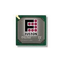
AFS250-FGG256 Actel, AFS250-FGG256 Datasheet - Page 100

AFS250-FGG256
Manufacturer Part Number
AFS250-FGG256
Description
FPGA - Field Programmable Gate Array 250K System Gates
Manufacturer
Actel
Datasheet
1.AFS600-PQG208.pdf
(330 pages)
Specifications of AFS250-FGG256
Processor Series
AFS250
Core
IP Core
Maximum Operating Frequency
1098.9 MHz
Number Of Programmable I/os
114
Data Ram Size
36864
Supply Voltage (max)
1.575 V
Maximum Operating Temperature
+ 70 C
Minimum Operating Temperature
0 C
Development Tools By Supplier
AFS-Eval-Kit, AFS-BRD600, FlashPro 3, FlashPro Lite, Silicon-Explorer II, Silicon-Sculptor 3, SI-EX-TCA
Mounting Style
SMD/SMT
Supply Voltage (min)
1.425 V
Number Of Gates
250 K
Package / Case
FPBGA-256
Lead Free Status / RoHS Status
Lead free / RoHS Compliant
Available stocks
Company
Part Number
Manufacturer
Quantity
Price
Company:
Part Number:
AFS250-FGG256
Manufacturer:
Actel
Quantity:
135
Company:
Part Number:
AFS250-FGG256
Manufacturer:
ACTEL
Quantity:
6 800
Company:
Part Number:
AFS250-FGG256I
Manufacturer:
Microsemi SoC
Quantity:
10 000
- Current page: 100 of 330
- Download datasheet (13Mb)
Device Architecture
Table 2-36 • Analog Block Pin Description (continued)
2- 84
Signal Name
AG6
AT6
ATRETURN67
AV7
AC7
AG7
AT7
AV8
AC8
AG8
AT8
ATRETURN89
AV9
AC9
AG9
AT9
RTCMATCH
RTCPSMMATCH
RTCXTLMODE[1:0]
RTCXTLSEL
RTCCLK
Analog Quad
With the Fusion family, Actel introduces the Analog Quad, shown in
basic analog I/O structure. The Analog Quad is a four-channel system used to precondition a set of
analog signals before sending it to the ADC for conversion into a digital signal. To maximize the
usefulness of the Analog Quad, the analog input signals can also be configured as LVTTL digital input
signals. The Analog Quad is divided into four sections.
The first section is called the Voltage Monitor Block, and its input pin is named AV. It contains a two-
channel analog multiplexer that allows an incoming analog signal to be routed directly to the ADC or
allows the signal to be routed to a prescaler circuit before being sent to the ADC. The prescaler can be
configured to accept analog signals between –12 V and 0 or between 0 and +12 V. The prescaler circuit
scales the voltage applied to the ADC input pad such that it is compatible with the ADC input voltage
range. The AV pin can also be used as a digital input pin.
The second section of the Analog Quad is called the Current Monitor Block. Its input pin is named AC.
The Current Monitor Block contains all the same functions as the Voltage Monitor Block with one
addition, which is a current monitoring function. A small external current sensing resistor (typically less
than 1 Ω) is connected between the AV and AC pins and is in series with a power source. The Current
Monitor Block contains a current monitor circuit that converts the current through the external resistor to
a voltage that can then be read using the ADC.
Number
of Bits
1
1
1
1
1
1
1
1
1
1
1
1
1
1
1
1
1
1
2
1
1
Direction
Output
Output
Output
Output
Output
Output
Output
Output
Input
Input
Input
Input
Input
Input
Input
Input
Input
Input
Input
Input
Input
R e visio n 1
Temperature monitor return shared by
Analog Quads 6 and 7
Analog Quad 7
Analog Quad 8
Temperature monitor return shared by
Analog Quads 8 and 9
Analog Quad 9
MATCH
MATCH connected to VRPSM
Drives XTLOSC RTCMODE[1:0] pins
Drives XTLOSC MODESEL pin
RTC clock input
Function
Figure 2-66 on page
Analog Quad
Analog Quad
Analog Quad
Analog Quad
Analog Quad
Analog Quad
Analog Quad
Analog Quad
Analog Quad
Analog Quad
Analog Quad
Analog Quad
Analog Quad
Analog Quad
Analog Quad
Analog Quad
Location of
2-85, as the
Details
RTC
RTC
RTC
RTC
RTC
Related parts for AFS250-FGG256
Image
Part Number
Description
Manufacturer
Datasheet
Request
R

Part Number:
Description:
FPGA 256/I�/Fusion Voltage: 1.5, 1.8, 2.5, 3.3 Mixed Voltage
Manufacturer:
Actel
Datasheet:

Part Number:
Description:
FPGA - Field Programmable Gate Array 250K System Gates
Manufacturer:
Actel
Datasheet:

Part Number:
Description:
MCU, MPU & DSP Development Tools Silicon Sculptor Programming Mod
Manufacturer:
Actel

Part Number:
Description:
MCU, MPU & DSP Development Tools InSystem Programming ProASICPLUS Devices
Manufacturer:
Actel

Part Number:
Description:
Programming Socket Adapters & Emulators PQ160 Module
Manufacturer:
Actel

Part Number:
Description:
Programming Socket Adapters & Emulators Axcelerator Adap Module Kit
Manufacturer:
Actel

Part Number:
Description:
Programming Socket Adapters & Emulators Evaluation
Manufacturer:
Actel

Part Number:
Description:
Programming Socket Adapters & Emulators AFDX Solutions
Manufacturer:
Actel

Part Number:
Description:
Programming Socket Adapters & Emulators SILICON SCULPTOR ADAPTER MODULE
Manufacturer:
Actel
Datasheet:

Part Number:
Description:
Programming Socket Adapters & Emulators Axcelerator Adap Module Kit
Manufacturer:
Actel

Part Number:
Description:
Programming Socket Adapters & Emulators Evaluation
Manufacturer:
Actel

Part Number:
Description:
Programming Socket Adapters & Emulators Silicon Sculptor Software
Manufacturer:
Actel

Part Number:
Description:
Programming Socket Adapters & Emulators InSystem Programming ProASICPLUS Devices
Manufacturer:
Actel


