BFR94A,215 NXP Semiconductors, BFR94A,215 Datasheet
BFR94A,215
Specifications of BFR94A,215


Related parts for BFR94A,215


BFR94A,215 Summary of contents
Page 1
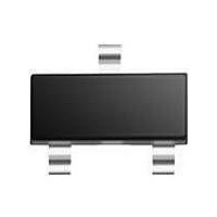
BFR94A NPN 5 GHz wideband transistor Rev. 3 — 15 November 2010 1. Product profile 1.1 General description NPN wideband transistor in a plastic SOT23 package. PNP complement; BFT92 1.2 Features and benefits High power gain Low noise figure Low ...
Page 2
... NXP Semiconductors 2. Pinning information Table 2. Pin Ordering information Table 3. Type number BFR94A 4. Marking Table 4. Type number BFR94A 5. Limiting values Table 5. In accordance with the Absolute Maximum Rating System (IEC 60134). V CBO V CEO V EBO tot T stg the temperature at the solder point of the collector pin. ...
Page 3
... NXP Semiconductors 6. Thermal characteristics Table 6. Symbol R th(j-sp) [ the temperature at the solder point of the collector pin Characteristics Table 7. Characteristics Symbol Parameter I collector-base cut-off current CBO h DC current gain FE C collector capacitance c C emitter capacitance e C feedback capacitance re f transition frequency T G unilateral power gain ...
Page 4
... NXP Semiconductors μH choke turns 0.4 mm copper wire, internal diameter 3 mm, winding pitch 1 mm. Fig 1. Intermodulation distortion and second harmonic distortion MATV test circuit 400 P tot (mW) 300 200 100 100 Fig 2. Power derating curve BFR94A Product data sheet 2 kΩ 300 Ω ...
Page 5
... NXP Semiconductors 1 (pF) 0.8 0.6 0 MHz Fig 4. Collector capacitance as a function of collector-base voltage; typical values 30 gain (dB 500 MHz. CE MSG = maximum stable gain. Fig 6. Gain as a function of collector current; typical values BFR94A Product data sheet 001aam886 (GHz ( °C. j Fig 5. 001aam888 ...
Page 6
... NXP Semiconductors 50 gain (dB MSG mA MSG = maximum stable gain maximum available gain. max Fig 8. Gain as a function of frequency; typical values (mS) 20 2.5 0 2.0 1.8 1.7 −20 − mA 800 MHz Fig 10. Circles of constant noise figure; typical values BFR94A Product data sheet 001aam890 gain ...
Page 7
... NXP Semiconductors 4 NF (dB Fig 12. Minimum noise figure as a function of collector current; typical values −45 IMD (dB) −50 −55 −60 −65 − Fig 14. Intermodulation distortion as a function of collector current; typical values BFR94A Product data sheet 001aam894 GHz 1 GHz 500 MHz (mA) C Fig 13. Minimum noise figure as a function of ...
Page 8
... NXP Semiconductors + j − mA Fig 16. Common emitter input reflection coefficient (S 180° mA Fig 17. Common emitter forward transmission coefficient (S BFR94A Product data sheet 1 0.5 0.2 1200 0.2 0 800 1000 500 200 0.2 0 Ω °C. O amb ); typical values 11 90° 120° 100 MHz 150° ...
Page 9
... NXP Semiconductors 180° mA Fig 18. Common emitter reverse transmission coefficient ( − mA Fig 19. Common emitter output reflection coefficient (S BFR94A Product data sheet 90° 120° 1200 MHz typ 150° 800 200 100 0 150° 120° −90° °C. amb 1 0.5 ...
Page 10
... NXP Semiconductors 8. Package outline Plastic surface-mounted package; 3 leads DIMENSIONS (mm are the original dimensions UNIT max. 1.1 0.48 0.15 mm 0.1 0.9 0.38 0.09 OUTLINE VERSION IEC SOT23 Fig 20. Package outline SOT23 BFR94A Product data sheet scale 3.0 1.4 2.5 1.9 0.95 2.8 1 ...
Page 11
... BFR94A v.3 20101115 • Modifications: The format of this data sheet has been redesigned to comply with the new identity guidelines of NXP Semiconductors. • Legal texts have been adapted to the new company name where appropriate. • Replaces previous data sheet and documentation of BFR94A. ...
Page 12
... In no event shall NXP Semiconductors be liable for any indirect, incidental, punitive, special or consequential damages (including - without limitation - lost profits, lost savings, business interruption, costs related to the removal or ...
Page 13
... NXP Semiconductors’ specifications such use shall be solely at customer’s own risk, and (c) customer fully indemnifies NXP Semiconductors for any liability, damages or failed product claims resulting from customer design and use of the product for automotive applications beyond NXP Semiconductors’ ...
Page 14
... NXP Semiconductors 13. Contents 1 Product profile . . . . . . . . . . . . . . . . . . . . . . . . . . 1 1.1 General description . . . . . . . . . . . . . . . . . . . . . 1 1.2 Features and benefits . . . . . . . . . . . . . . . . . . . . 1 1.3 Applications . . . . . . . . . . . . . . . . . . . . . . . . . . . 1 1.4 Quick reference data . . . . . . . . . . . . . . . . . . . . 1 2 Pinning information . . . . . . . . . . . . . . . . . . . . . . 2 3 Ordering information . . . . . . . . . . . . . . . . . . . . . 2 4 Marking . . . . . . . . . . . . . . . . . . . . . . . . . . . . . . . . 2 5 Limiting values Thermal characteristics . . . . . . . . . . . . . . . . . . 3 7 Characteristics . . . . . . . . . . . . . . . . . . . . . . . . . . 3 8 Package outline . . . . . . . . . . . . . . . . . . . . . . . . 10 9 Abbreviations . . . . . . . . . . . . . . . . . . . . . . . . . . 11 10 Revision history . . . . . . . . . . . . . . . . . . . . . . . . 11 11 Legal information ...