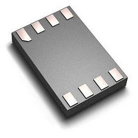
NX3L1T53GT,115 NXP Semiconductors, NX3L1T53GT,115 Datasheet
NX3L1T53GT,115
Specifications of NX3L1T53GT,115


Related parts for NX3L1T53GT,115


NX3L1T53GT,115 Summary of contents
Page 1
NX3L1T53 Low-ohmic single-pole double-throw analog switch Rev. 04 — 24 March 2010 1. General description The NX3L1T53 is a low-ohmic single-pole double-throw analog switch suitable for use as an analog or digital 2:1 multiplexer/demultiplexer. It has a digital select input ...
Page 2
... NXP Semiconductors 3. Applications Cell phone PDA Portable media player 4. Ordering information Table 1. Ordering information Type number Package Temperature range Name −40 °C to +125 °C NX3L1T53GT −40 °C to +125 °C NX3L1T53GD −40 °C to +125 °C NX3L1T53GM 5. Marking [1] Table 2. Marking codes Type number ...
Page 3
... NXP Semiconductors 6. Functional diagram Fig 1. Logic symbol Fig 2. Logic diagram 7. Pinning information 7.1 Pinning NX3L1T53 GND 3 GND 4 Transparent top view Fig 3. Pin configuration SOT833-1 (XSON8) NX3L1T53_4 Product data sheet Low-ohmic single-pole double-throw analog switch 001aad386 001aaj537 Fig 4. Rev. 04 — 24 March 2010 ...
Page 4
... NXP Semiconductors Fig 5. Pin configuration SOT902-1 (XQFN8U) 7.2 Pin description Table 3. Pin description Symbol Pin SOT833-1 and SOT996 GND 3 GND Functional description [1] Table 4. Function table Input [ HIGH voltage level LOW voltage level don’t care. NX3L1T53_4 Product data sheet Low-ohmic single-pole double-throw analog switch ...
Page 5
... NXP Semiconductors 9. Limiting values Table 5. Limiting values In accordance with the Absolute Maximum Rating System (IEC 60134). Voltages are referenced to GND (ground = 0 V). Symbol Parameter V supply voltage CC V input voltage I V switch voltage SW I input clamping current IK I switch clamping current SK I switch current ...
Page 6
... NXP Semiconductors 11. Static characteristics Table 7. Static characteristics At recommended operating conditions; voltages are referenced to GND (ground 0 V). Symbol Parameter Conditions V HIGH-level input voltage LOW-level input voltage input leakage select input S and enable ...
Page 7
... NXP Semiconductors 11.1 Test circuits − Fig 6. Test circuit for measuring OFF-state leakage current − Fig 7. Test circuit for measuring ON-state leakage current 11.2 ON resistance Table 8. ON resistance At recommended operating conditions; voltages are referenced to GND (ground = 0 V); for graphs see ...
Page 8
... NXP Semiconductors Table 8. ON resistance …continued At recommended operating conditions; voltages are referenced to GND (ground = 0 V); for graphs see Symbol Parameter ΔR ON resistance mismatch ON between channels R ON resistance (flatness) V ON(flat) [1] Typical values are measured at T [2] Measured at identical V , temperature and input voltage. CC [3] Flatness is defined as the difference between the maximum and minimum value of ON resistance measured at identical V temperature ...
Page 9
... NXP Semiconductors ( °C. Measured at T amb Fig 9. ON resistance as a function of input voltage 1 (Ω) 1.2 0.8 0 125 °C. (1) T amb = 85 °C. (2) T amb = 25 °C. (3) T amb = −40 °C. (4) T amb Fig 10. ON resistance as a function of input voltage 1.5 V ...
Page 10
... NXP Semiconductors 1 (Ω) 0.8 0.6 0.4 0 125 °C. (1) T amb = 85 °C. (2) T amb = 25 °C. (3) T amb = −40 °C. (4) T amb Fig 12. ON resistance as a function of input voltage 2 1 (Ω) 0.8 0.6 0.4 0 125 °C. (1) T amb = 85 °C. (2) T amb = 25 °C. (3) T amb = − ...
Page 11
... NXP Semiconductors 12. Dynamic characteristics Table 9. Dynamic characteristics At recommended operating conditions; voltages are referenced to GND (ground = 0 V); for load circuit see Symbol Parameter Conditions t enable time Yn; en see t disable time Yn; dis see t break-before-make see b-m time [1] Typical values are measured at T [2] Break-before-make guaranteed by design. ...
Page 12
... NXP Semiconductors 12.1 Waveform and test circuits S, E input output OFF to HIGH HIGH to OFF output HIGH to OFF OFF to HIGH Measurement points are given in Logic levels: V and Fig 16. Enable and disable times Table 10. Measurement points Supply voltage 4.3 V NX3L1T53_4 Product data sheet ...
Page 13
... NXP Semiconductors a. Test circuit b. Input and output measurement points Fig 17. Test circuit for measuring break-before-make timing V Test data is given in Table Definitions test circuit Load resistance Load capacitance including jig and probe capacitance External voltage for measuring switching times. EXT V may be connected ...
Page 14
... NXP Semiconductors Table 11. Test data Supply voltage 4.3 V 12.2 Additional dynamic characteristics Table 12. Additional dynamic characteristics At recommended operating conditions; voltages are referenced to GND (ground = 0 V); V ≤ specified 2.5 ns amb Symbol Parameter THD total harmonic distortion −3 dB frequency f (−3dB) response α ...
Page 15
... NXP Semiconductors 12.3 Test circuits V IL Fig 19. Test circuit for measuring total harmonic distortion V IL Adjust f voltage to obtain 0 dBm level at output. Increase f i Fig 20. Test circuit for measuring the frequency response when switch is in ON-state Adjust f voltage to obtain 0 dBm level at input. ...
Page 16
... NXP Semiconductors a. Test circuit b. Input and output pulse definitions V may be connected Fig 22. Test circuit for measuring crosstalk voltage between digital inputs and switch Fig 23. Test circuit for measuring crosstalk NX3L1T53_4 Product data sheet Low-ohmic single-pole double-throw analog switch logic input 0.5V ...
Page 17
... NXP Semiconductors a. Test circuit b. Input and output pulse definitions = ΔV × inj O L ΔV = output voltage variation generator resistance. gen V = generator voltage. gen V may be connected Fig 24. Test circuit for measuring charge injection NX3L1T53_4 Product data sheet Low-ohmic single-pole double-throw analog switch ...
Page 18
... NXP Semiconductors 13. Package outline XSON8: plastic extremely thin small outline package; no leads; 8 terminals; body 1 x 1. 8× (2) terminal 1 index area DIMENSIONS (mm are the original dimensions) ( UNIT b D max max 0.25 2.0 mm 0.5 0.04 0.17 1.9 Notes 1. Including plating thickness. 2. Can be visible in some manufacturing processes. ...
Page 19
... NXP Semiconductors XSON8U: plastic extremely thin small outline package; no leads; 8 terminals; UTLP based; body 0.5 mm terminal 1 index area DIMENSIONS (mm are the original dimensions) A UNIT max 0.05 0.35 2.1 mm 0.5 0.00 0.15 1.9 OUTLINE VERSION IEC SOT996 Fig 26. Package outline SOT996-2 (XSON8U) ...
Page 20
... NXP Semiconductors XQFN8U: plastic extremely thin quad flat package; no leads; 8 terminals; UTLP based; body 1.6 x 1.6 x 0.5 mm terminal 1 index area metal area not for soldering 2 1 terminal 1 index area DIMENSIONS (mm are the original dimensions) A UNIT max 0.05 0.25 1.65 mm 0.5 0.00 ...
Page 21
... NXP Semiconductors 14. Abbreviations Table 13. Abbreviations Acronym Description CDM Charged Device Model CMOS Complementary Metal-Oxide Semiconductor ESD ElectroStatic Discharge HBM Human Body Model MM Machine Model 15. Revision history Table 14. Revision history Document ID Release date NX3L1T53_4 20100324 NX3L1T53_3 20100201 • Modifications: Section • Table ...
Page 22
... In no event shall NXP Semiconductors be liable for any indirect, incidental, punitive, special or consequential damages (including - without limitation - lost profits, lost savings, business interruption, costs related to the removal or ...
Page 23
... NXP Semiconductors 17. Contact information For more information, please visit: For sales office addresses, please send an email to: NX3L1T53_4 Product data sheet Low-ohmic single-pole double-throw analog switch http://www.nxp.com salesaddresses@nxp.com Rev. 04 — 24 March 2010 NX3L1T53 © NXP B.V. 2010. All rights reserved ...
Page 24
... NXP Semiconductors 18. Contents 1 General description . . . . . . . . . . . . . . . . . . . . . . 1 2 Features . . . . . . . . . . . . . . . . . . . . . . . . . . . . . . . 1 3 Applications . . . . . . . . . . . . . . . . . . . . . . . . . . . . 2 4 Ordering information . . . . . . . . . . . . . . . . . . . . . 2 5 Marking . . . . . . . . . . . . . . . . . . . . . . . . . . . . . . . . 2 6 Functional diagram . . . . . . . . . . . . . . . . . . . . . . 3 7 Pinning information . . . . . . . . . . . . . . . . . . . . . . 3 7.1 Pinning . . . . . . . . . . . . . . . . . . . . . . . . . . . . . . . 3 7.2 Pin description . . . . . . . . . . . . . . . . . . . . . . . . . 4 8 Functional description . . . . . . . . . . . . . . . . . . . 4 9 Limiting values Recommended operating conditions Static characteristics 11.1 Test circuits . . . . . . . . . . . . . . . . . . . . . . . . . . . . 7 11.2 ON resistance . . . . . . . . . . . . . . . . . . . . . . . . . . 7 11 ...