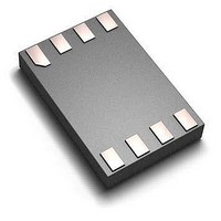
74LVC1G74GF,115 NXP Semiconductors, 74LVC1G74GF,115 Datasheet - Page 11

74LVC1G74GF,115
Manufacturer Part Number
74LVC1G74GF,115
Description
IC FLIP-FLOP SGL D S/R XSON8
Manufacturer
NXP Semiconductors
Datasheet
1.74LVC1G74DC125.pdf
(25 pages)
Specifications of 74LVC1G74GF,115
Number Of Circuits
1
Logic Family
74LVC1G74
Logic Type
Positive Edge Triggered Single D Flip Flop
Propagation Delay Time
4.1 ns, 5.9 ns, 7.1 ns, 13.4 ns
Supply Voltage (max)
5.5 V
Maximum Operating Temperature
+ 125 C
Mounting Style
SMD/SMT
Package / Case
XSON-8
Minimum Operating Temperature
- 40 C
Supply Voltage (min)
1.65 V
Lead Free Status / RoHS Status
Lead free / RoHS Compliant
Other names
568-5456-2
NXP Semiconductors
12. Waveforms
Table 10.
74LVC1G74
Product data sheet
Supply voltage
V
1.65 V to 1.95 V
2.3 V to 2.7 V
2.7 V
3.0 V to 3.6 V
4.5 V to 5.5 V
Fig 8.
CC
Measurement points are given in
The shaded areas indicate when the input is permitted to change for predictable output performance.
V
The clock input (CP) to output (Q, Q) propagation delays, the clock pulse width, the D to CP set-up, the
CP to D hold times and the maximum frequency
OL
Measurement points
and V
OH
are typical output voltage levels that occur with the output load.
CP input
Q output
Q output
D input
GND
GND
V
V
V
V
Table
OH
OH
OL
OL
V
V
Input
V
0.5 × V
0.5 × V
1.5 V
1.5 V
0.5 × V
All information provided in this document is subject to legal disclaimers.
I
I
M
10.
V
M
t
PLH
CC
CC
CC
t
Single D-type flip-flop with set and reset; positive edge trigger
su
Rev. 9 — 5 August 2010
t
V
h
M
V
V
M
M
t
PHL
1/f
max
t
W
t
PHL
t
su
t
h
Output
V
0.5 × V
0.5 × V
1.5 V
1.5 V
0.5 × V
M
mnb141
t
PLH
CC
CC
CC
74LVC1G74
© NXP B.V. 2010. All rights reserved.
11 of 25


